- Mark as New
- Bookmark
- Subscribe
- Mute
- Subscribe to RSS Feed
- Permalink
- Report Inappropriate Content
With a very simple circuit the outputs of an EPM3064ATC44 are very noisy, see attachment. The 1 kHz clock is visible on the outputs with very high needle pulses. These pulses are similarly on all 7 outputs.
The circuit is a 4bit counter, 74161, connected to a BCD to 7segment decoder, 7448.
The input is a 1 kHz clock (pin37).
The outputs of the decoder are connected to pins 12,13,14,15, 18, 19,20.
All VCC pins of the chip (3.3 V) are blocked with 100 nF to ground.
The EPM3064A is the only chip on my test board.
Is 100 nF too small? What can I do to get clear outputs?
BTW, the outputs are wrong. They do not show correct 7 segment numbers (on a state analyzer). Simulation within Quartus II showed correct outputs. I guess that the heavy noise causes the errors.
Link Copied
- Mark as New
- Bookmark
- Subscribe
- Mute
- Subscribe to RSS Feed
- Permalink
- Report Inappropriate Content
Without seeing your schematic and PCB layout it is hard to make any significant comments. That being said:
What does your input clock signal look like? Is it monotonic with no noise?
Can you zoom in on a transition on the data? Interesting to see what an output transition looks like in detail.
What does the power rail look like, wrt noise?
I have multiple EPM7064S and EPM3064A parts on boards (using PLCC packaging) and don't see such issues.
- Mark as New
- Bookmark
- Subscribe
- Mute
- Subscribe to RSS Feed
- Permalink
- Report Inappropriate Content
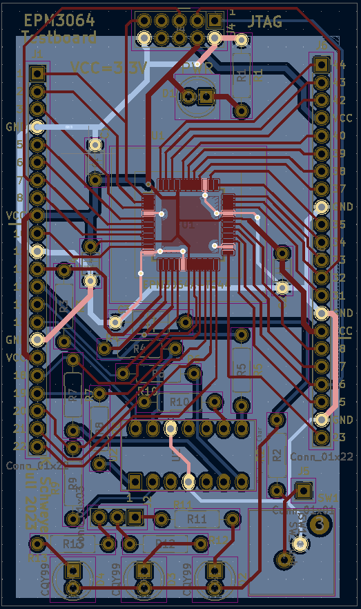
You can find the schematic and the layout in the attachment.
In the layout I planned to use a socket for the EPM3064 chip. I found a small one in the internet, but it does not meet the specified dimensions of a TQFP44 chip. With the socket the chip cannot be programmed at all.
Therefore I made a second version with the chip soldered directly on the board. For the tests I only mounted the chip, the JTAG socket, the 4 blocking capacitors and some pins for power supply and input/outputs.
The layout is shown in a version with highlighted ground and VCC.
- Mark as New
- Bookmark
- Subscribe
- Mute
- Subscribe to RSS Feed
- Permalink
- Report Inappropriate Content
Well, the schematic looks ok, the PCB layout is what I would consider less than optimal.
But it appears you are using a two layer board, so not much flexibility to provide solid power/ground to a TQFP SMT device.
That being said, you still need to provide waveforms for your power rail and the clock input signal.
You don't indicate how the 1KHz clock input is being generated and any noise on it will of course cause false triggering like you see.
--
I have my EPM3064A PLCC44 development/test board I did, but I included a three terminal 5V to 3.3V regulator on the board.
Power is supplied by a 5V USB connector (no USB, just power). I do have a bulk 10uF caps on the 3.3V regulator output and input.
My board has a socket for a 4pin DIP oscillator; currently I am using a 50MHz 3.3V CMOS oscillator.
A significant difference however is I used a 4 layer board design, with a full ground plane, and split 3.3V/5V power plane.
Signals are all routed on either top or bottom.
A simple test program I use in the 3064A is a series of binary counters, 54 bits in total, driving some discrete LEDS.
A total of 60 registers and all 64 macrocells are used.
The test code runs just fine at 50MHz; Quartus says the -7 part should run at an Fmax of 68.49MHz.
Output signals are clean and the counters operate reliably.
- Mark as New
- Bookmark
- Subscribe
- Mute
- Subscribe to RSS Feed
- Permalink
- Report Inappropriate Content
besides improving the layout, if glitches are produced by a combinational decoder, it can help to modify the design so that the all output are registered.
- Mark as New
- Bookmark
- Subscribe
- Mute
- Subscribe to RSS Feed
- Permalink
- Report Inappropriate Content
Meanwhile I tested various changes, but the spikes on the outputs are still there. I added 100 uF between the power pins but no influence on 1 kHz spikes.
Now I can provide some more images.
- clock1kHz.png: CLK input from test output of my oscilloscope, amplitude reduced by serial resistor and parallel zener diode
- clock1kHz_zoomed.png: positive edge of CLK input zoomed
- VCC-AC.png: VCC with AC coupling to oscilloscope, CLK input connected
- VCC-AC-noOsci.png: same as above but Oscilloscope disconnected (only ground is connected). As can be seen, some 1kHz noise is picked up in my test configuration.
When CLK input is disconnected all spikes on VCC are gone.
With every positive edge of CLK the chip seems to sink a lot of current which cannot be provided by the capacitors. Generally this means that every synchronous design will suffer from this effect. The more macrocells a design uses the more severe these effects will be.
On my fully equiped testboard there is a 7 segment display with common cathode, i.e. the outputs of EPM3064A have to provide current to the LEDs in the display. This might increase the problem with spikes.
Is EPM3064A suitable for a synchronous design?
Are there chips which are better with respect to current spikes?
- Mark as New
- Bookmark
- Subscribe
- Mute
- Subscribe to RSS Feed
- Permalink
- Report Inappropriate Content
The EPM3K/7K series are absolutely suitable for synchronous design. I have used them in that way for years with clock rates from 10MHz up to 50MHz.
The noise spikes on the clock edges are not unexpected, as current will be drawn during signal transitions. Unfortunately the spikes will be exaggerated in your design because of the poor quality of your power distribution. Your traces on the two layer board will be highly inductive and are causing this noise to be generated on the power rails. Depending on your LED series resistor values you might also see high current draw (which in an inductive environment causes ringing) from the LED currents.
For reference, my test board designs for the EPM7064S and EPM3064A series PLCC44 parts use a four layer design with full power and ground planes under the device. Local 10uF bulk decoupling. No individual 100nF devices. Using a 50MHz CMOS oscillator and a design which has 60 registers and 64 macrocells as three simultaneous 18b binary counters I see no more than 100mV of noise on the power rail (5V or 3.3V as applicable to the device).
Also, on your BCD to seven segment decoder outputs, they are not synchronous, it is just logic, so expect to see switching noise on the edges as the 4b synchronous counter values propagates thru the logic. They may bounce up and down for 10 to 20ns after each clock edge. That is expected for non registered outputs.
PS: one additional thought ... what type of probing arrangement did you use on your scope to capture the waveforms?
I am guessing it is a probably 10X scope probe and there is a ground lead of 10cm or so in length that you connected to a ground point.
If so, this can add additional ringing on the measured signal due to the probing ground loop (it is inductive) that is not really there.
Ideally you would use a probe with an adjacent 2.5mm or so ground connection clip so there is no long ground loop connection.
Just thought I would ask ...
- Mark as New
- Bookmark
- Subscribe
- Mute
- Subscribe to RSS Feed
- Permalink
- Report Inappropriate Content
Thank you telling me about your experience and examples.
What is your opinion about the chances to achieve good results with a 2 layer design and wider power rails?
Do you know or hear about successful 2 layer designs with EPM3064A?
If not all pins of the chip are used, VCC power rails can be made wider. And a ground plane like in my layout always is possible.
- Mark as New
- Bookmark
- Subscribe
- Mute
- Subscribe to RSS Feed
- Permalink
- Report Inappropriate Content
I have done two layer designs using the EPM7032S and EPM7064S parts in the PLCC44 package in thru hole sockets.
They worked fine. The boards were all done with thru hole parts so it was easy enough to provide power using 25 to 50 mil traces.
I have not done two layer boards using the TQFP44 packages; those have all been four layer designs with a power/ground plane.
Most all the other components were surface mount as well, and the layout packed pretty tight. The added cost (basically a 4 layer board is 2X the cost of a 2 layer board) for a small prototype board in the 50mm x 100mm range was acceptable.
Using power and ground islands under the TQFP package, and multiple small vias for connecting the power pins to the islands should be achievable. But you need to implement the power/ground solution first, and then squeeze in the signal traces after.
- Subscribe to RSS Feed
- Mark Topic as New
- Mark Topic as Read
- Float this Topic for Current User
- Bookmark
- Subscribe
- Printer Friendly Page