- Mark as New
- Bookmark
- Subscribe
- Mute
- Subscribe to RSS Feed
- Permalink
- Report Inappropriate Content
Hello,
I'm having problems achieving the 64 bytes/cycle L2 to L1 cache bandwidth on the Haswell core. I can only achieve 32 bytes/cycle. Does anyone know if this is possible? Several other reviewers on the web are having the same problem. Was this a typo on the Intel slides for Haswell? My current code is using integer loads. Is the claimed 64 bytes/cycle dependent on SSE loads? I'm stumped.
Thanks,
Stephen
Tom's hardware:
L1D, L2, and L3 cache bandwidth are all up on our Core i7-4770K compared to my preview piece. However, only the L1D yields the doubling of bandwidth we were expecting. Given 64 bytes/cycle (compared to 32 for Ivy Bridge), this number should still be much higher than it is.
http://www.tomshardware.com/reviews/core-i7-4770k-haswell-review,3521-12.html
We’re surprised that the L2 cache is just 7% faster on Haswell, but the massive L1 bandwidth is a huge jump.
Link Copied
- Mark as New
- Bookmark
- Subscribe
- Mute
- Subscribe to RSS Feed
- Permalink
- Report Inappropriate Content
The Haswell core can only issue two loads per cycle, so they have to be 256-bit AVX loads to have any chance of achieving a rate of 64 Bytes/cycle.
- Mark as New
- Bookmark
- Subscribe
- Mute
- Subscribe to RSS Feed
- Permalink
- Report Inappropriate Content
Thanks for the comment John. I will try using 256 bit AVX loads.
My current program is just doing a DWORD load with a stride of 64 bytes. Naturally, this is a fake benchmark, but in theory it should be loading a 64 byte line into the L1 from the L2 each clock. For some reason the code can't get past the 32 bytes / clock rate. What surprises me even more is that I can't find any benchmark or article that demonstrates the Haswell cpu running at 64 bytes / clock from the L2. Not one.
Now, if Haswell can achieve 64 bytes / clock with two 256 AVX loads, then why not with a single DWORD load with a 64 byte stride? This might imply that the L2/L1 logic is somehow coupled with the AVX unit and not the integer unit. That would be really strange.
Anyhow, I will give it a try with AVX loads. I welcome any help in figuring this out.
Thanks again,
Stephen
- Mark as New
- Bookmark
- Subscribe
- Mute
- Subscribe to RSS Feed
- Permalink
- Report Inappropriate Content
How the DWORD stride is loaded? Are AVX registers or 64-bit GP register used to load the data?
- Mark as New
- Bookmark
- Subscribe
- Mute
- Subscribe to RSS Feed
- Permalink
- Report Inappropriate Content
Thanks for asking Iliyapolak, Here is the basic loop for my integer code. It is just a simple load and increment pointer that repeats thirty-two times. In theory the haswell core should be able to do a load every clock. Each load should bring in 64 bytes / cycle, but it doesn't. It is taking two clocks per load just like Ivy Bridge or Sandy Bridge.
I will implement an AVX version on Monday.
Thanks,
Stephen
//* Load 256k minus 32k into L2 *//
//* Then touch the oldest 32k * 4 again *//
mov ecx, 32k * 4
mov esi, BUFFER
top:
mov eax, dword [esi]
add esi, 64
//* The MOV, ADD sequence repeats 32 times *//
sub ecx, (64 * 32)
jne top:
- Mark as New
- Bookmark
- Subscribe
- Mute
- Subscribe to RSS Feed
- Permalink
- Report Inappropriate Content
>>> In theory the haswell core should be able to do a load every clock>>>
I think that load of 64 bytes per clock can be achieved with the help of AVX registers only. I only suppose that at level of the internal implementation when load mov instructions are stored inside Load buffer their targets or data is loaded into physical registers waiting probably for AGU to calculate store address and send the data to L1D Cache. I do not know if the problem is related to number of physical integer registers which are loaded with the data. I was thinking about the possibility that internally data is transfered by 32-bit physical registers and hence lower bandwith per cycle
- Mark as New
- Bookmark
- Subscribe
- Mute
- Subscribe to RSS Feed
- Permalink
- Report Inappropriate Content
There is absolutely no doubt that you can only move 64 Bytes per cycle into registers by using AVX instructions. There are very clearly only 2 load units (ports 2 and 3 shown in Figure 2-1 of the Intel Architectures Optimization Manual, document 248966-030, September 2014), so only two load uops can be executed per cycle. The biggest load payload is 256 bits == 32 Bytes, and 64 Bytes / 2 loads = 32 Bytes per load.
If you assume that whole cache lines are being transferred between the L1 and L2, then you can compute a "hardware bandwidth" by multiplying the number of L1 misses/second by 64 Bytes/miss. Since this approach does not concern itself with getting data all the way into registers, you can use any type of load to generate the misses. Implementation recommendations:
- A stride of 64 Bytes for reads on a data structure that is larger than L1 cache and smaller than L2 cache should give an L1 miss every cycle.
- When using small (4KiB) pages, the random mapping of virtual to physical addresses will mean that you can't count on retaining data structures that are the full size of the L2. Fortunately the L1 is well-behaved, so you actually only need to access a data structure that is slightly larger than the L1 to get it to completely flush every time through. 64 KiB is a good size for flushing the L1 cache without too much risk of missing the L2. (Using 2MiB pages eliminates this problem.)
- You will want ignore the timings the first time through the measurement, since they will be contaminated by both L2 misses and by writebacks of dirty data from the L1.
- Inline RDTSC or RDTSCP instructions should be used for timing, and the loop should be sized so that the overhead of these timer reads (typically ~30-35 cycles, but I have not tested this on Haswell) is negligible.
- Check the assembly code to make sure that there are not extraneous instructions that could cause pipeline bubbles. I usually make sure the loop is unrolled a few times.
- Mark as New
- Bookmark
- Subscribe
- Mute
- Subscribe to RSS Feed
- Permalink
- Report Inappropriate Content
I suppose that at the hardware level physical AVX registers could be using multiplexed 256-bit wide paths to the Load/Store ports hence the 64-byte/cycle bandwitdh. In the case of physical GP registers 64-bit width path can be probably used to transfer multiplexed data hence the lower bandwidth.
- Mark as New
- Bookmark
- Subscribe
- Mute
- Subscribe to RSS Feed
- Permalink
- Report Inappropriate Content
Unfortunately Intel has not disclosed enough of the details of their cache implementation to guide the development of L2 cache bandwidth benchmarks. I have some ideas, but not enough time to implement and test them...
I think it is safe to assume that Intel is telling the truth when they say that Haswell can transfer 64 Bytes per cycle from the L2 to the L1 -- but that is only a very small part of the story! Moving data from the L2 cache to the L1 data cache is always associated with motion of data from the L1 data cache to the core, and it is not at all clear how these transfers interact. For example on Sandy Bridge (where I have done most of my testing), we know that the L1 data cache is composed of 8 banks, each handling accesses to a different 8 Byte field of a 64-byte cache line, and each capable of handling only one read access per cycle.. The L2 to L1 interface is reported to be capable of delivering 32 Bytes per cycle, but we don't know if the data is delivered as writing to four consecutive banks on each of two cycles, or if it writes to all eight banks every other cycle. Even for "read-only" access patterns the data must be written into the L1 data cache, and we don't know how the L1 data cache banks handle the mixture of reads (to the core) and writes (incoming data from the L2). We don't know if a demand load bringing data from the L2 to the L1 data cache bypasses that data to the core (thus eliminating the need to read the data from the L1 data cache), but if L1 hardware prefetch is active then at least some of the lines being read from L2 to L1 will get there in advance of the demand load which, so those will have to be read from the L1.
The situation is more complex if the core is performing both reads and writes. Timing issues might be critical, and timing is extremely difficult to control if there are any stores in the instruction stream. It is also not clear how reads and writes interact in the L1 data cache banks, and not clear how L1 writebacks to the L2 and L1 refills from the L2 interact with L1 cache reads and writes. Do L1 writebacks (which are reads of the L1 cache array) conflict with (i.e. use the same read ports as) reads from the core? Does the writeback access all 8 L1 data cache banks for one cycle or four banks in each of two cycles? Performance in the presence of writebacks might be strongly impacted by the existence of small "victim buffers" between the L1 and L2 caches (to prevent conflicts between the victim write and the incoming data read, which always go to the same cache set).
For Haswell the cache organization has clearly changed, but the descriptions don't go into enough detail to understand how the L2 to L1 transfers will interact with L1 to core transfers. The result may eventually be easier to understand than the banked L1 on Sandy Bridge, but there are lots of possible implementations and it is very hard to design microbenchmarks to disambiguate across the possibilities. It is also likely that the real implementation is more complex than any hypothesis that an outside party is likely to come up with, which would result in either a "false positive" in the microbenchmark testing, or a set of results that is inconsistent with any of the proposed models.
- Mark as New
- Bookmark
- Subscribe
- Mute
- Subscribe to RSS Feed
- Permalink
- Report Inappropriate Content
The 64 bytes/cycle represents the data bus width from the L2->L1. That is doubled over prior generations @ 32 bytes/cycle. The sustained BW from L2->L1 is less than this peak capability but is also nearly doubled on Haswell over prior generations.
Vish
- Mark as New
- Bookmark
- Subscribe
- Mute
- Subscribe to RSS Feed
- Permalink
- Report Inappropriate Content
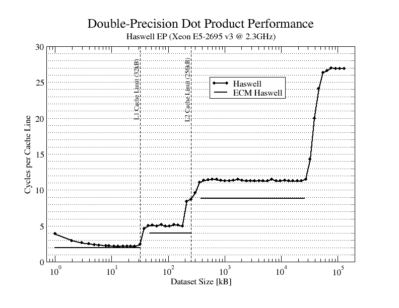
Our investigations of Haswell indeed indicate that it is possible to achieve a bandwidth of more than 32B/c (about 43B/c) from L2 to L1 in load-only scenarios. This is under the assumption that the L1 is single-ported, i.e. data can only be transfered from L2 to L1 in cycles that don't overlap with data transfers from L1 to registers. In the attached plot you can see that that it takes approximately two cycles to compute the dot product for one cache line with data residing in L1 (two vfmadds, four vmovpds taking two cycles with two avx loads happening each cycle).
With data residing in the L2 cache, we'd expect a total of four clock cycles (two additional cycles to transfer two cache lines from L2 to L1), but we actually see about three (or less in the case of Broadwell) cycles, which corresponds to something in the ballpark of 40B/c.
However, for streaming access patterns that involve evicts from L1 to L2 I observed the bandwidth degrades to 32B/c. I've read somewhere that the L1-L2 eviction bandwidth is only 32B/c, but still this should result in a 'mixed' bandwidth higher than 32B/c depending on the load to evict ratio, e.g. for a copy-a-to-b-kernel: load a (43B/c), write-allocate b (43B/c), evict b (32B/c) should yield an average L2 bandwidth of 39B/c. Can someone comment on that?
- Mark as New
- Bookmark
- Subscribe
- Mute
- Subscribe to RSS Feed
- Permalink
- Report Inappropriate Content
Hi Johannes,
Could you post the code for your ddot_fma kernel here?
Thanks
- Mark as New
- Bookmark
- Subscribe
- Mute
- Subscribe to RSS Feed
- Permalink
- Report Inappropriate Content
Hi Johannes,
Could you post the code for your ddot_fma kernel here?
Thanks
- Mark as New
- Bookmark
- Subscribe
- Mute
- Subscribe to RSS Feed
- Permalink
- Report Inappropriate Content
The source code would be interesting, as there are factors besides L2 bandwidth which could limit performance of fma dot product. For example, gcc gives better performance without fma, as lack of "riffling" makes the overall latency of fma the limiting factor.
One may doubt whether plain dot products are included in the mix of application kernels which would have motivated the increased bandwidth between L2 and L1 implemented in Haswell. Parallel dot products, as in dgemm, might be among the motivators, but those allow for L1 locality of at least one operand.
- Mark as New
- Bookmark
- Subscribe
- Mute
- Subscribe to RSS Feed
- Permalink
- Report Inappropriate Content
I finally got around to looking at the attached charts and realized that I am confused....
The chart shows performance approaching 2 cycles "per cache line" for the largest L1-containable sizes. Assuming that "per cache line" means "for processing 8 FMAs" (i.e., reading one cache line from each of the two input vectors), this corresponds to a bandwidth of 128 Bytes in 2 cycles, or 64 Bytes/cycle, which is the expected value for a core that can execute 2 32-Byte loads per cycle.
Moving to L2-contained data, the chart shows that the performance is bounded below by 5 cycles "per cache line". This is only 40% of the performance of the L1-contained version, so it corresponds to a sustained rate of 25.6 Bytes/cycle. This is only 40% of the stated L2-L1 bandwidth of 64 Bytes/cycle, and 20% lower than the peak 32 Bytes/cycle of the previous generation.
Assuming that the L1 Data Cache is "single ported" (i.e., it can either provide data to the core or receive refills from the L2 in any cycle) should result in a 4-cycle minimum time "per cache line" -- 2 cycles to execute the 4 loads to move the 128 Bytes from the L1 Data Cache to the core plus 2 cycles to move two new lines from the L2 cache to the L1 Data Cache.
Looking at the chart, I don't see any evidence of execution in less than 5 cycles -- every data point from 40 KiB to ~120 KiB is at or above 5 cycles. This suggests that in addition to being "single ported", there is at least one additional cycle required in this access pattern, and it is hard to understand why such an overhead would be required. (With stores and writebacks it is pretty easy to come up with scenarios that should result in such delays.)
So I finally see where the "43 Bytes/cycle" mentioned above comes from -- it *assumes* that the L1 can only provide data to the core or receive data from the L2 in any cycle, and then derives an average L2 to L1 rate based on the excess cycles -- 128 Bytes in 3 excess cycles is 42.67 Bytes/cycle. I think it is important to be clear that the "43 bytes/cycle" is not a measurement, but an interpretation based on what is almost certainly an oversimplified model of the actual implementation. The measurement is 25.6 Bytes per cycle for the DDOT kernel operating with data that is expected to be in the L2 cache. There may be other, more obscure, explanations for the discrepancy between this value and the 64 Byte/cycle burst rate claimed for the L2 to L1 interface.
These numbers are very close to 2x faster than the previous generation of products, but they are still disappointing. The L1-contained DDOT takes 2 cycles and requires 2 4-wide FMAs, so it is running at 1/2 the peak arithmetic rate of the chip. The L2-contained DDOT drops this from 50% of peak (8 FLOPS/cycle) to 20% of peak (3.2 FLOPS/cycle), which could be provided by an SSE implementation with separate 128-bit FP add and FP multiply units running at 20% lower frequency -- comparable to technology released by Intel 13-14 years ago.
- Mark as New
- Bookmark
- Subscribe
- Mute
- Subscribe to RSS Feed
- Permalink
- Report Inappropriate Content
I notice the assembler above uses 32 bit instructions and registers. DWORD is 32 bit AFAIK for historical reasons. I would try using 64 bit registers (rax, etc). I think the assembler is smart enough to use the correct 64 bit bit ops, but to be sure use explicit 64 bit ops such as loadq.
I think the data bus is still 64 bits, please correct me if I am wrong.
Benchmarking 64 bit vs 128 bit sse4.x ( xmm0 and such) loads, I see these not being any faster than the 64 bit loads. That would point to the data bus being 64 bit wide.
- Mark as New
- Bookmark
- Subscribe
- Mute
- Subscribe to RSS Feed
- Permalink
- Report Inappropriate Content
For what it's worth, if you disable the "L2 hardware prefetcher" (i.e, bit 0 in MSR 0x1A4 as described here), you can potentially achieve much higher L2 bandwidths for codes contained entirely in L2 which have a streaming pattern, at least on the Skylake system I tested (which likely has a similar L2 configuration to Haswell).
With a simple forward load pattern with stride 64, and L2 prefetcher disabled, I was able to get 1.12 cycles / load, giving an implied bandwidth from L2 of ~57 bytes/cycle. At least we can see here that the L1 can apparently accept a line from L2 and satisfy a load instruction in the same cycle (at least for most cycles).
With the L2 prefetcher enabled, I was only able to get a load every 1.65 cycles approximately (these measurements had more variance) for a much lower implied bandwidth of 38 bytes/cycle.
Using perf counters l2_rqsts.references and l2_rqsts.pf_hit I was able to confirm that the L2 prefetcher was causing a large number of additional references to L2, which evidently complete with the real work the L2 is doing.
My interpretation is the L2 prefetcher (which only brings stuff into L2 or L3) is monitoring the accesses to L2 and detects the stream and then probes the L2 to see if the next line(s) are there. In this benchmark, they always are, so no downwards request to L3 occurs, but the simple act of probing uses L2 resources. That's news to me: I was certainly aware that prefetching could be detrimental in cases where you unnecessarily brought lines in that won't be used, but that's not happening here but PF has a large cost. In other L2-contained tests where there was more than 1 stream the effect was even more pronounced (approaching a 2x degradation).
Something to keep in mind if you have L2-heavy loads.
- Mark as New
- Bookmark
- Subscribe
- Mute
- Subscribe to RSS Feed
- Permalink
- Report Inappropriate Content
My notes above from 2015-08-08 (https://software.intel.com/en-us/forums/software-tuning-performance-optimization-platform-monitoring/topic/532346#comment-1834608) were never updated to reflect the additional testing I did on the Haswell processors. These additional tests were in agreement with Travis's comments.
Specifically:
- Haswell performance when streaming data from the L2 cache is consistent with a 64-Byte L2 -> L1 interface, but with an L1 Data Cache that can only talk to the core or the L2 in any cycle.
- This makes the peak effective bandwidth 32 Bytes per cycle, and this is reflected in the newer versions of the Intel Optimization Reference Manual (e.g., Table 2-1 in document 248966-037 refers to the Broadwell L2 cache bandwidth as 32 Bytes/cycle "max" and 25 Bytes/cycle "sustained".
- Disabling the L2 HW prefetchers improved the sustained L2 bandwidth slightly for my read-only kernel, but I was unable to get noticeably more than 80% of 32 Bytes/cycle.
- With the L2 HW prefetchers enabled, performance varied significantly from iteration to iteration. As Travis notes, in any cycle, the L2 cache can service a request from the L1 or it can probe the tags for an L2 prefetch, but not both. About 1/2 of the L2 HW prefetches appear to delay servicing an L1 load request for one cycle, but the number of L2 HW prefetches varied dramatically from iteration to iteration -- from near zero to near 100% of the lines being loaded. I eventually tracked this variability down, and showed that when the processor exits the scheduler interrupt (typically every millisecond), the L2 HW prefetcher is very aggressive. In subsequent iterations, the L2 HW prefetcher becomes less aggressive, allowing demand loads to consume more of the cycles. Then the next interrupt occurs and the cycle starts over again.
- The new version of the Optimization Reference manual (248966-037, Table 2-1) says that the Skylake Server processor has twice the maximum L2 bandwidth of the Broadwell processor -- 64 Bytes/cycle "max" instead of 32, with 52 Bytes/cycle "sustained" instead of 25.
- This could be due to changes in the L1 or in the L2.
- More ports on the L1 Data Cache could allow L2 to core loads at 64 Bytes/cycle, even with no change to the L2 interface.
- More ports on the L2 Data Cache (allowing two 64-bit cache line fills per cycle) could also allow 64 Bytes/cycle. E.g., in cycle 0, transfer 128 Bytes from L2 to L1, then in cycle 1 the core performs two 64-Byte loads from L1, for an average peak bandwidth of 128 bytes/2 cycles = 64 Bytes/cycle.
- It is easy to imagine that L2 HW prefetches would conflict with L1 misses in the same was as they do on Haswell.
- This could be due to changes in the L1 or in the L2.
- Mark as New
- Bookmark
- Subscribe
- Mute
- Subscribe to RSS Feed
- Permalink
- Report Inappropriate Content
@Dr. McCalpin:
To be clear, I'm testing on Skylake-client (aka SKL) not server (aka SKX). My assumption is that the L2 design for HSW, BDW and SKL (client) is similar, so I was implying that results on SKL apply also to Haswell. The optimization manual and promotional materials don't really indicate any bit improvement for the L1/L2 cache interface - they list BDW, HSW and SKL all at 64 "peak bandwidth" and at 25 and ~29 "sustained" respectively for BDW and SKL (no figure given for HSW).
In any case, you mention: Haswell performance when streaming data from the L2 cache is consistent with a 64-Byte L2 -> L1 interface, but with an L1 Data Cache that can only talk to the core or the L2 in any cycle.
However, my test of a simple stride-by-64 QWORD byte read:
top:
mov rax, [rdx]
add  rdx, 64
sub rcx, 1
jne top
Runs in about 1.1 cycles per iteration. This must bring in a cache line iteration, so this means that on most (9 out of 10) cycles the L1D must be accepting a line from L2 the cache and satisfying the read from the core. That means that the idea that the L1 can only do one of those things seems incorrect at least on Skylake client (if someone has Haswell, I'd like to see your results). This result holds for 16 and 32 byte reads too, at any alignment that doesn't cross a cache line. Of course, this shows that you can achieve nearly 64 byte bandwidth from L2 to L1, but we aren't using all the data.
If you add a second read to the above loop, to the same cache line, even to the same location, I can never get better than 2 cycles per iteration (I get close, about 2.05 cycles). So it seems the L1D can satisfy a load from L2, and a load from the core, but not a second load from the core in the same cycle. I'm not sure why: one idea is perhaps the load from L2 requires a read port on the L1D, so there is only one other read port for up to one read from the core. It seems like loads should only need the write port though, but maybe it needs the read port in the case of evicting a line at the same time?
FWIW my full load-64 byte test (two 32 byte loads) runs at 2.05 cycles which is a sustained bandwidth of 31.2 byte/cycle, actually a bit better than the Intel guide's ~29 (I'm not doing much with the data though!). Perhaps they were testing with prefetch on: with prefetch I get about 28 bytes/cycle.
I eventually tracked this variability down, and showed that when the processor exits the scheduler interrupt (typically every millisecond), the L2 HW prefetcher is very aggressive. In subsequent iterations, the L2 HW prefetcher becomes less aggressive, allowing demand loads to consume more of the cycles. Then the next interrupt occurs and the cycle starts over again.<blockquote>
This is really interesting. Thanks for sharing! Do you think it is an intentional design, where essentially the return from an interupt is heuristically seen as a good time to be more aggressive (since the interrupt may have blown away some of the cache or switched processes and so now is a really good time to try to fill the caches again with relevant data), or just an outcome of the general heuristics interacting with the code in interrupt? I would guess the latter: when your L2-bound kernel is running for a while perhaps the L2 prefetcher eventually realizes that it's always already getting hits in L2, so just chills out, but then whatever happens in interrupt resets this - perhaps the prefetcher state micro-architecturally doesn't survive interrupts or ring transitions, or perhaps the interrupt code just causes the prefetcher to start tracking other streams and it forgets what it learned about your kernel's L2 stream. In any case it's some steam in the sails of "tickless" kernels.
- Mark as New
- Bookmark
- Subscribe
- Mute
- Subscribe to RSS Feed
- Permalink
- Report Inappropriate Content
Thanks for the clarification -- I wondered if you might be referring to the Skylake client, but did not remember long enough to mention it...
The Haswell L2 HW prefetch behavior is almost certainly just a side effect of the heuristics used. It looks like the L2 HW prefetcher is aggressive when the L2 access rate is low (or when the L2 miss queue is lightly populated), and backs off when the L2 access rate high (or the L2 miss queue gets close to full). This is consistent with the few words that Intel has published on the topic. It seems plausible to assume that the scheduler interrupt handler creates a low L2 cache access rate, so the HW prefetcher will naturally be most aggressive when it sees new data streams after returning from that interrupt handler. What I don't understand is why it takes so long for the L2 HW prefetcher to realize that the L2 cache is really busy servicing L1 requests and decide that it should back off. Reading a 64 KiB array from the L2 cache at 25 Bytes/cycle only takes 2620 cycles, or about 1 microsecond. So I can run almost 1000 of these iterations in the time between to ticks of the 1 millisecond scheduler interrupt, and in most cases it takes most of these iterations before the L2 HW prefetcher actually backs off significantly.
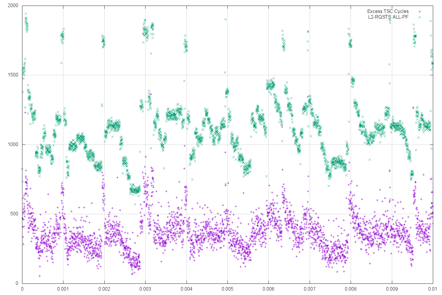
The attached file shows a series of these L2 read bandwidth results from a Xeon E5-2690 v3 (Haswell EP) system.
- The x axis is wall-clock time in seconds.
- The purple "+" symbols are the "excess" TSC cycles required to complete each iteration.
- "Excess" is relative to my best measured time of 7540 cycles (=> 26.1 Bytes/cycle).
- The average "excess TSC" cycles is about 400, corresponding to about a 5% slowdown relative to the best result.
- The worst "excess TSC" values are in the 750 cycle range, corresponding to a 10% slowdown.
- The green "x" symbols show the L2_RQSTS.ALL_PF counts (Event 0x24, Umask 0xF8).
- These show a huge spike every millisecond.
- The most common pattern shows a decay until the next millisecond "spike", but there are many irregularities.
- The processor frequency was pinned to the nominal 2.6 GHz frequency, so TSC and core cycle counts are the same.
- This figure shows 10 milliseconds pulled from a 62 millisecond run -- the remainder shows similar behavior, but makes the plot even harder to read.
On Sandy Bridge this highly variable behavior of the L2 HW prefetcher is similar (in particular, L2 prefetches are issued for all streams, even if there are never any L2 misses), but since the L2 cache requires 2 cycles to deliver a line to the L1 cache, there is always an alternate cycle in which the prefetcher can query the L2 tags without interfering with accesses from the L1 Data Cache. So the L2 HW prefetches don't result in noticeable performance variation. Even on Haswell, you have to be running the L2 interface at very close to 100% utilization before the HW prefetches interfere with L2 hits enough to make a noticeable performance difference. This is easy to do with microbenchmarks, but seems quite unlikely with a real application. Stores almost certainly change the picture as well, but it is much harder to create controlled experiments that have a mix of loads and stores, so I have not done much in that direction (for L2-contained data).
- Subscribe to RSS Feed
- Mark Topic as New
- Mark Topic as Read
- Float this Topic for Current User
- Bookmark
- Subscribe
- Printer Friendly Page