I am working on a project related to completion detection in asynchronous circuits and I have chosen the Altera FPGA as my test platform. The decision to use the Altera platform is that it is the most costs effective platform but I would need to constraint the synthesis tool to behave in a particular manner and is hoping you would be able to provide some pointer/guidance.
I am now making my design using schematic entry instead of Verilog/VHDL and I have noticed that the delay from all inputs to all outputs has the same delay as the synthesis tool would have optimized the design into possible a single logic element or a LUT. What I was hoping to do, just because I want to prove some theorem, is to constraint the synthesis tool to not optimize the design and to keep every logic element in the schematic entry as a separate logic element on its own in the final implementation. A friend who is using XILINX said there is this DONT_TOUCH or KEEP attribute that will do what I am asking for and is wondering if there is something similar in Altera that we could use. If there is, what is the Altera equivalent and how would we set this, please?
連結已複製
Hi,
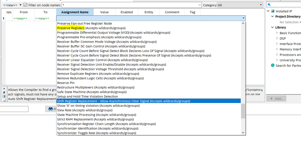
In the Intel Quartus Prime software, you can use keep/preserve synthesis attribute in the HDL (VHDL attribute / Verilog attribute) but not in schematic. If you would like to preserve the register, you may do so by using the Assignment Editor - 'Preserve Registers'. This assignment prevents a register from minimizing away during synthesis and prevents sequential netlist optimization.
Thanks
Best regards,
KhaiY
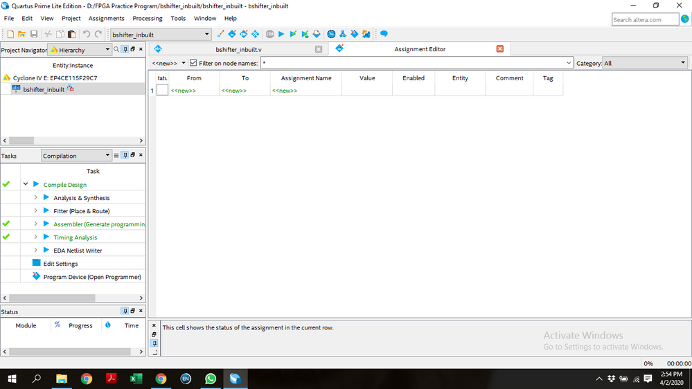
Thank you for your reply KhaiY. Could you please assist me how can I keep/preserve synthesis attribute in the Verilog language? I am a beginner in FPGA and Quartus, and I am not familiar with the basics of using it. One more thing, when I follow the path Assignment-->Assignment Editor, I am not getting 'Preserve Registers' option. I have shared the screenshot of what I can see after selecting Assignment editor. I would be grateful if you can help me out.
I am using Quartus Prime Lite Edition.
Regards
Pallavi
Hi Pallavi,
You may find the example of usign preserve in Verilog here:
https://www.intel.com/content/www/us/en/programmable/quartushelp/17.0/hdl/vlog/vlog_file_dir_preserve.htm
Besides this, you may find the preserve register assignment in the dropdown menu in Assignment Editor
Thanks.
Best regards,
KhaiY
Thank you for your reply. I am actually working on FPGA and constructed a barrel shifter in .bdf (block diagram/ schematic file). I have used the DE2 115 board. A barrel shifter shifts the data logarithmically; to shift n-bit data, log n (base 2) stages are required. For example, for an 8-bit barrel shifter, 3 stages S2, S1 and S0 are required which can shift the data by 4 bit (or no shift), 2bit (or no shift) and 1 bit (or no shift) respectively. The combination of stages can shift an 8-bit data from 0 to 7 bits. The shifter is designed by using 2x1 Muxes with 3 stages, 8 mux per stage and the shift amount is given by the select lines of each stage.
In my design, I have connected the 8-bit data (to be shifted) and the select lines S2, S1, and S0 (to provide the shift amount) with the switches on the FPGA board, and the output (i.e. data after shifting) is connected to red LEDs. Now I need to calculate the time taken by the shifter to shift the data as soon as I flip the switch position. I have tried using DSO to calculate the timing, Channel 1 of DSO connected to one of the switches used for select lines ( S2, S1 or S0 ) and Channel 2 of DSO is connected to one of the LEDs used for output. The expected outcome was:
If the time taken by a single stage of shifter is "t", then the time taken by two stages would be "2t" and time taken by three stages would be "3t". However, when I captured the waveform on DSO for different stages of shifter, it is showing a constant time for all the stages.
i) To shift an 8-bit data by 1 bit, a single stage would be used. (Flip only Switch S0 from off to on, S1 and S2 are off)
Channel 1 of DSO connected to S0, Channel 2 of DSO is connected to LEDR0. Only one stage is used. The time difference between flipping S0 input and changing LEDR0 from 0 to 1 is around 20ns.
ii) To shift an 8-bit data by 2 bit, a two stages would be used. (Flip only Switch S1 from off to on, S0 and S2 are off)
Channel 1 of DSO connected to S1, Channel 2 of DSO is connected to LEDR0. Two stages are used. The time difference between flipping S1 input and changing LEDR0 from 0 to 1 is around 20ns. It was expected to be approx 40ns.
iii) To shift an 8-bit data by 4 bit, a three stages would be used. (Flip only Switch S2 from off to on, S1 and S0 are off)
Channel 1 of DSO connected to S2, Channel 2 of DSO is connected to LEDR0. Three stages are used. The time difference between flipping S2 input and changing LEDR0 from 0 to 1 is around 20ns. It was expected to be approx 60ns.
I assume that this constant delay is a predefined delay, and if I can use something to constraint the synthesis tool to not optimize the design and to keep every logic element in the schematic entry as a separate logic element on its own in the final implementation, then maybe I will be able to capture the time taken by each stage of the shifter. Could you please suggest whether my approach is right or not?
Hi
I have used schematic entry because I am not very comfortable with HDL language. However, I can convert the schematic entry into an HDL language. I have done that already, and now my question is how to use the keep/preserve in the HDL file. I am using the quartus lite version, can I use the keep/preserve or I need to use the paid version of Quartus prime software?
Hi,
You can use preserve/keep in the Lite edition. You may find the example of usign preserve in Verilog here:
https://www.intel.com/content/www/us/en/programmable/quartushelp/17.0/hdl/vlog/vlog_file_dir_preserve.htm
VHDL:
https://www.intel.com/content/www/us/en/programmable/quartushelp/current/index.htm#hdl/vhdl/vhdl_file_dir_preserve.htm
Thanks.
Best regards,
KhaiY

