- Mark as New
- Bookmark
- Subscribe
- Mute
- Subscribe to RSS Feed
- Permalink
- Report Inappropriate Content
Hi,
I’m setting up a design in Quartus 18.0 for Cyclone V 5CGTFD9E5F35I7 using two LPDDR2 hard memory controllers:
- TOP: 40bit LPDDR2 Hard Memory Controller
- BOT: 32bit LPDDR2 Hard Memory Controller
Both hard memory controllers are instantiated in Platform Designer and the memory pins are connected to the top level design directly.
During fitting I got the following error:
I found the following article:
https://www.intel.com/content/www/us/en/programmable/support/support-resources/knowledge-base/solutions/rd11152012_357.html
For me, it is not clear, how to write the assignment?
- What did they mean with “<variation name>”?
- Do I have to write the same assignment for hard memory controller TOP and BOTTOM?
- Do I set this as value, or do I need also a tag?
Thanks for your assistance!
Link Copied
- Mark as New
- Bookmark
- Subscribe
- Mute
- Subscribe to RSS Feed
- Permalink
- Report Inappropriate Content
Hi DB,
I assume you are placing the DM pin according to the respective DQS group. The DM pin need to place to the same group like DQS. For example, DM[0] need to place to same x8 DQ group of DQS[0].
What is meant by the <variation name> is the hierarchy path of the termination control block in your project.
Assuming all the DM pin placement is correct then I suspect the Quartus Error (175005) is due to a known issue problem in the Quartus II software version 12.1 and later. If more than one UniPHY-based memory controller is instantiated without OCT sharing, the fitter may assign some pins for every interface to one OCT control block. This will cause errors because only one OCT control block can drive a I/O bank.
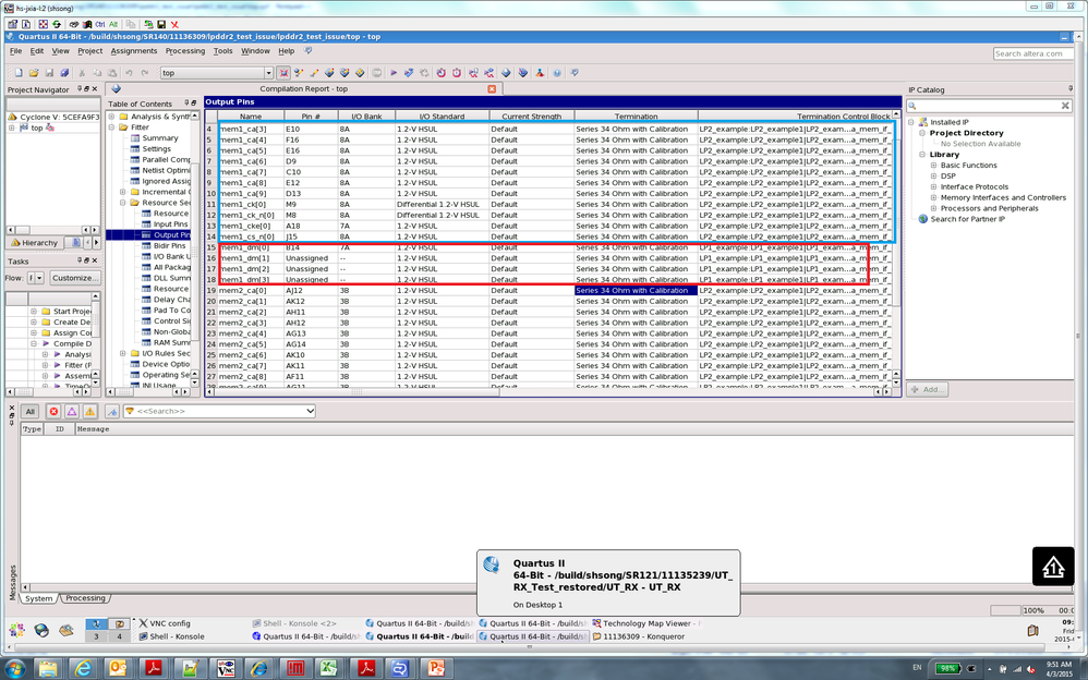
To verify if this is the issue, in the Compilation Report, go to Fitter -> Resource Section -> Output pins and scroll to the row with the mem_* signal. Scroll to the right and verify which OCT control block the pin is assigned to.
I attach the screenshots of the example report here for your reference. You can see fitter assign some mem1_* signals(mem1_ca[*],mem1_ck*, etc.) to
termination control block in LP2_example_xxxx(highlighted in blue). Since there is no oct sharing, all the mem1_* pins should use termination control block in LP1_example_xxx.
As a workaround, please add following assignments in the QSF and re-compile your project and fitter can pass.
set_instance_assignment -name TERMINATION_CONTROL_BLOCK "LP1_example:LP1_example1|LP1_example_if0:if0|altera_mem_if_oct_cyclonev:oct0|sd1a_0" -to mem1_ca[*]
set_instance_assignment -name TERMINATION_CONTROL_BLOCK "LP1_example:LP1_example1|LP1_example_if0:if0|altera_mem_if_oct_cyclonev:oct0|sd1a_0" -to mem1_ck[0]
set_instance_assignment -name TERMINATION_CONTROL_BLOCK "LP1_example:LP1_example1|LP1_example_if0:if0|altera_mem_if_oct_cyclonev:oct0|sd1a_0" -to mem1_ck_n[0]
set_instance_assignment -name TERMINATION_CONTROL_BLOCK "LP1_example:LP1_example1|LP1_example_if0:if0|altera_mem_if_oct_cyclonev:oct0|sd1a_0" -to mem1_cke[0]
set_instance_assignment -name TERMINATION_CONTROL_BLOCK "LP1_example:LP1_example1|LP1_example_if0:if0|altera_mem_if_oct_cyclonev:oct0|sd1a_0" -to mem1_cs_n[0]
Again, this is just an example project. You should follow the hierarchy path based on your current project.
Hope this helps. 😊 Let me know if you have any concern.
Regards,
NAli1
- Mark as New
- Bookmark
- Subscribe
- Mute
- Subscribe to RSS Feed
- Permalink
- Report Inappropriate Content
Hi NAli1,
thanks for your assistance!
I adapted the assignements to my design for both LPDDR2 memories, top and bottom.
Now it works and the fitter runs successful.
Thanks!
Best regards
DB
- Mark as New
- Bookmark
- Subscribe
- Mute
- Subscribe to RSS Feed
- Permalink
- Report Inappropriate Content
Hi DB,
Glad to know everything is working at your side now .😊 You are more than welcome .
Regards,
NAli1
- Subscribe to RSS Feed
- Mark Topic as New
- Mark Topic as Read
- Float this Topic for Current User
- Bookmark
- Subscribe
- Printer Friendly Page

