- 신규로 표시
- 북마크
- 구독
- 소거
- RSS 피드 구독
- 강조
- 인쇄
- 부적절한 컨텐트 신고
hi. i try to store sine wave into dual port RAM. However , the output of RAM, q is 1 cycle slower. when i count, i already include 1 cycle for output registered. May i know why?
i change the configuration of RAM without output registered, the output is still the same(suppose the output should 1 cycle faster) The functional simulation of it is attached. thanks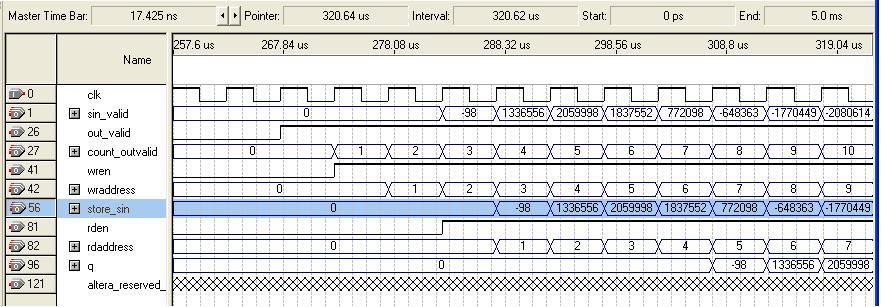
링크가 복사됨
- 신규로 표시
- 북마크
- 구독
- 소거
- RSS 피드 구독
- 강조
- 인쇄
- 부적절한 컨텐트 신고
It looks like you are registering the read address so it takes 1 cycle to clock the internal ram address, then the read data is valid on the second cycle, in effect a 1 stage pipeline.
My design is not ready yet for simulation, so please post the results if you remove the external register. My whole design depends on the 1 cycle access so I am very interested in your results!!!!!- 신규로 표시
- 북마크
- 구독
- 소거
- RSS 피드 구독
- 강조
- 인쇄
- 부적절한 컨텐트 신고
I see q changes -98 1 cycle after read address 3m w/o output registered.
Read address 3 is 2 cycles after write address 3, was it supposed to be 1 cycle later instead of 2?- 신규로 표시
- 북마크
- 구독
- 소거
- RSS 피드 구독
- 강조
- 인쇄
- 부적절한 컨텐트 신고
"I see q changes -98 1 cycle after read address 3m w/o output registered."
When clock trigger, store_sin is 0 due to delay of fsin_o. So, the DRAM, save the 0 instead of -98 at address 3. However, i still have some question on the wo output registered. It is because i find out that q is immediate changing(few ns delay) instead of clock triggering for a simple design. Any idea on this? "Read address 3 is 2 cycles after write address 3, was it supposed to be 1 cycle later instead of 2?" You are right if you want read the data immediately and it actually depends on the application that when to read the data.- 신규로 표시
- 북마크
- 구독
- 소거
- RSS 피드 구독
- 강조
- 인쇄
- 부적절한 컨텐트 신고
I think that inside the memory the address is latched not registered which means the address flushes through the latch while the clock is high and on through the decoders then on to q. The latches are then held when the clock is low so that q can be registered at the next clock and the delay through the ram provides the hold time for the register. q async changes shortly after the clock. (The time is the ram access time)
So the address in can come from a posedge register, flush thru the latches and decoders then on to produce q async (wo reg). The latches are then held until the next clock when the the operation repeats. The path length is ram access time + external logic delay for any logic driven by q.- 신규로 표시
- 북마크
- 구독
- 소거
- RSS 피드 구독
- 강조
- 인쇄
- 부적절한 컨텐트 신고
May i know that the content stored in RAM is saved in a file? Is it possible to retrieve?
I understand that the content can be retrieved from the simulation result. However, it is not an efficient process since any signal change will be recorded. thanks- 신규로 표시
- 북마크
- 구독
- 소거
- RSS 피드 구독
- 강조
- 인쇄
- 부적절한 컨텐트 신고
When clock trigger, store_sin is 0 due to delay of fsin_o. So, the DRAM, save the 0 instead of -98 at address 3.
I disagree because when address 3 is read, the q value is -98 as it should be