- Mark as New
- Bookmark
- Subscribe
- Mute
- Subscribe to RSS Feed
- Permalink
- Report Inappropriate Content
I can see from this thread that a differential (LVDS) EMIF PLL reference clock is only supported in LVDS I/O banks (and not 3 V I/O banks) in Arria 10:
https://community.intel.com/t5/Programmable-Devices/Is-LVDS-supported-on-the-dedicated-clock-input-of-the-Cyclone-10/td-p/270112
However, synthesis fails even if I follow this rule for the EMIF's "address and command bank", but try to use a 3 V I/O bank for the EMIF's "data bank":
This error occurs even after I have stripped down my pin assignments to the absolute minimum. I only constrain the LVDS PLL reference clock to be in Bank 2K (which is an LVDS bank) and I constrain just one data bit to be in Bank 2L (which is a 3 V I/O bank). No other pin constraints are defined:
I have carefully followed the "I/O Bank Usage" guidelines on p. 17 of "External Memory Interfaces Intel Arria 10 FPGA IP User Guide):
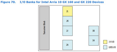
I have carefully checked the I/O bank types on p. 105 of "Intel Arria 10 Core Fabric and General Purpose I/Os Handbook":
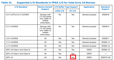
I have carefully checked Table 33 on p. 101 of the same document, which indicates that SSTL-15 should be supported in 3 V I/O banks:
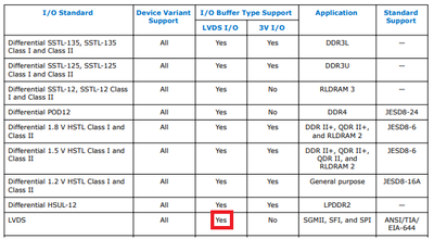
And, on p. 102, LVDS should be supported in LVDS I/O banks:
Therefore, I don't understand why this doesn't work.
As a first sanity check, I have confirmed that constraining the data pins to be in I/O Bank 2J (an LVDS bank) synthesizes without error:
What am I missing here? Is there some way to avoid this synthesis error?
- Mark as New
- Bookmark
- Subscribe
- Mute
- Subscribe to RSS Feed
- Permalink
- Report Inappropriate Content
@AdzimZM_Intel My understanding from the documentation is that disabling all the on-chip termination damages performance.
Since it is so difficult to get clear and reliable information from Intel (and so much time has already been wasted in this pursuit), we decided to redesign our hardware to use a single-ended reference clock.
Link Copied
- « Previous
-
- 1
- 2
- Next »
- Mark as New
- Bookmark
- Subscribe
- Mute
- Subscribe to RSS Feed
- Permalink
- Report Inappropriate Content
The example design is a design that has been generated by the Quartus software.
The design contains the components that are needed for the IP in order to work.
The point that I showed you in the example design is by changing the FPGA I/O termination, you should be able to use 3V I/O bank.
The A10 EMIF handbook has stated this configuration.
In your design, the top level file needs to edit because one signal has been disable from the EMIF IP.
It's oct signal. By disabling oct signal in your top level file, your design can be compiled.
I will attached the your design later.
Regards,
Adzim
- Mark as New
- Bookmark
- Subscribe
- Mute
- Subscribe to RSS Feed
- Permalink
- Report Inappropriate Content
The attachment is your design.
I have disable the oct signal in your top level file.
- Mark as New
- Bookmark
- Subscribe
- Mute
- Subscribe to RSS Feed
- Permalink
- Report Inappropriate Content
@AdzimZM_Intel My understanding from the documentation is that disabling all the on-chip termination damages performance.
Since it is so difficult to get clear and reliable information from Intel (and so much time has already been wasted in this pursuit), we decided to redesign our hardware to use a single-ended reference clock.
- Mark as New
- Bookmark
- Subscribe
- Mute
- Subscribe to RSS Feed
- Permalink
- Report Inappropriate Content
Hello and Good day!
Do you have any update upon your testing?
If yes, then may I know the feedback?
Thank you.
Regards,
Adzim
- Mark as New
- Bookmark
- Subscribe
- Mute
- Subscribe to RSS Feed
- Permalink
- Report Inappropriate Content
We do not receive any response from you to the previous reply that I have provided. This thread will be transitioned to community support. If you have a new question, feel free to open a new thread to get the support from Intel experts. Otherwise, the community users will continue to help you on this thread. Thank you.
- Mark as New
- Bookmark
- Subscribe
- Mute
- Subscribe to RSS Feed
- Permalink
- Report Inappropriate Content
There are some constraints that are not immediately apparent from the reference material. One thing is that the DQS pins may only go on certain pins, and that the data pins associated with that DQS pin must be in the same "pin-group" as the DQS. This is due to the hard controller having fixed assignments. The Pin Planner's "DQS" legend is badly wrong and most of the documentation is confusing at best.
In Pin Planner, go to View/Show/Show DQ-DQS pins/your mode (x4, x8, etc). Note the color blocks. Similarly for the command pins, which are also forced, at least if you are using the hard controller. This allowed me to get LPDDR3 to fit.
- Mark as New
- Bookmark
- Subscribe
- Mute
- Subscribe to RSS Feed
- Permalink
- Report Inappropriate Content
Also the attached file for command line pinouts, which MUST be on specific pins
- Subscribe to RSS Feed
- Mark Topic as New
- Mark Topic as Read
- Float this Topic for Current User
- Bookmark
- Subscribe
- Printer Friendly Page
- « Previous
-
- 1
- 2
- Next »


