- Mark as New
- Bookmark
- Subscribe
- Mute
- Subscribe to RSS Feed
- Permalink
- Report Inappropriate Content
Dear community,
I'm using the avalon-mm Interface and would like to determine the link width of the PCIe connection.
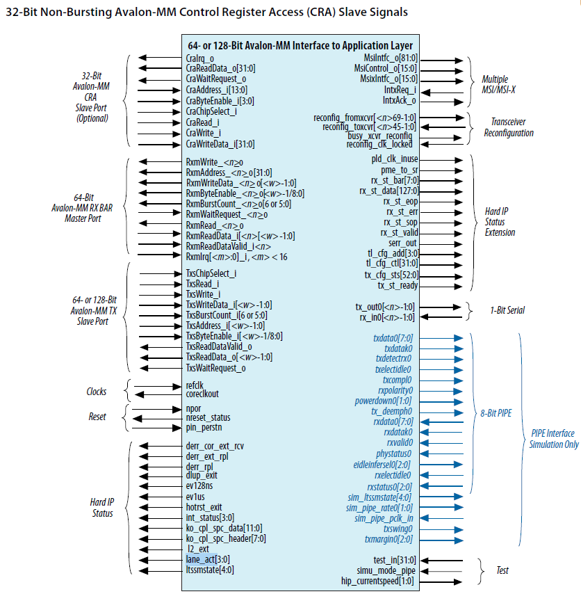
Can I access the link width via some register shown in the figure below - maybe - lane_act?
I read that the link width is set during the configuration phase of link training. There is a ltssmstate register, but how to use it for my purpose is not clear to me.
Has anyone done this before?
I would be grateful for any advice.
Best regards
Figure:
Link Copied
- Mark as New
- Bookmark
- Subscribe
- Mute
- Subscribe to RSS Feed
- Permalink
- Report Inappropriate Content
Hi Sir
Yes you can use Signaltap to monitor the value of lane_act to determine the link width.
While LTTSSM signal is to determine the PCIe link up (01111: L0 indicate the PCIe link is established and stable, other than L0 state means the PCIe link is not up).
Definition of these signals from the PCIe User Guide.
In between, below link have some PCIe Reference Designs that would be useful as reference.
- Mark as New
- Bookmark
- Subscribe
- Mute
- Subscribe to RSS Feed
- Permalink
- Report Inappropriate Content
Dear skbeh,
thank you very much for the hint.
I succeeded to determine the link width just by reading the lane_act register, because the register retains its value even after the training phase. I did not yet managed to use the ltssm register.
A few more questions:
1) Why ltssm = "01111" - isn't it the recovery state?
2) What exactly is L0 and which register can i read it from?
3) When exactly does the training phase take place, when the card is powered via the PCIe slot and programmed with a sof file?
Is it directly after programming?
Best regards
- Mark as New
- Bookmark
- Subscribe
- Mute
- Subscribe to RSS Feed
- Permalink
- Report Inappropriate Content
Please see inline replies below.
1) Why ltssm = "01111" - isn't it the recovery state?
>> It depends on which FPGA device you are using. I'm not sure you are using which fpga. For Arria 10 it is 5’b 01111, Stratix 10 it is 6'h11: S_L0
You can refer to the appropriate pcie user guides below which have the encoding definition.
https://www.intel.com/content/www/us/en/support/programmable/support-resources/design-guidance/pcie-support.html
2) What exactly is L0 and which register can i read it from?
>> ltssmstate is the top-Level signal at the PCIe core that can be used for debugging purpose. Also can be found in the respective user guides above.
3) When exactly does the training phase take place, when the card is powered via the PCIe slot and programmed with a sof file? Is it directly after programming?
>> After programmed the .sof, a PC reboot is required to force system enumeration/link training to discover the PCIe device.
Recommended you refer to application note AN690 at https://www.intel.com/content/dam/www/programmable/us/en/pdfs/literature/an/an690.pdf
See section '1.6.3. Installing the Hardware'.
- Subscribe to RSS Feed
- Mark Topic as New
- Mark Topic as Read
- Float this Topic for Current User
- Bookmark
- Subscribe
- Printer Friendly Page
