- Mark as New
- Bookmark
- Subscribe
- Mute
- Subscribe to RSS Feed
- Permalink
- Report Inappropriate Content
I am using a Cyclone 5CGXFC5C7F23C8N in a new design and planning to implement a PCIe x4 endpoint with CvP enabled.
The CVP user guide, UG-01101, states that I need to use the bottom left hard IP with the nPERSTL1 as the PCIe reset for CVP.
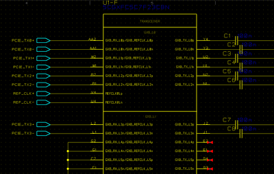
If this is the case then which of the 6 transceiver channels do I need to connect my 4 data lanes to ? Is the bottom left hard IP core associated with L0 or L1? Or does it not work in this way?
Link Copied
- Mark as New
- Bookmark
- Subscribe
- Mute
- Subscribe to RSS Feed
- Permalink
- Report Inappropriate Content
Hi,
You should be using using L0 with Ch0 - Ch3 connected. Please refer to https://www.intel.co.jp/content/dam/altera-www/global/ja_JP/pdfs/literature/ug/ug_c5_pcie.pdf Figure 7-38
- Mark as New
- Bookmark
- Subscribe
- Mute
- Subscribe to RSS Feed
- Permalink
- Report Inappropriate Content
Thanks John, I have connected as shown below. Using Ch3 in L1 as the 4th lane. Is this correct?
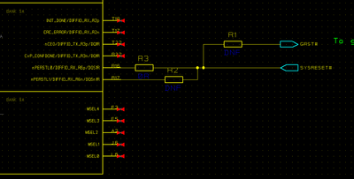
Also, should I use nPERSTL0 or L1 ?
Many Thanks
Frank
- Mark as New
- Bookmark
- Subscribe
- Mute
- Subscribe to RSS Feed
- Permalink
- Report Inappropriate Content
Hi,
The transceiver pin looks good to me. You will need to use nPERSTL1 pin as this is the use for CvP.
- Mark as New
- Bookmark
- Subscribe
- Mute
- Subscribe to RSS Feed
- Permalink
- Report Inappropriate Content
Thank you John.
I am now looking at what config scheme is best for me alongside CvP.
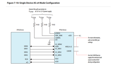
I am planning to use AS x4 with a EPCQ device for the periphery image for my Cyclone V GX, as below:
I have 2 questions:
What is the best way to program the EPCQ? I want to use the ByteBlaster interface, do I need to connect it to the AS interface rather than to the Cyclone's JTAG pins (via SFL bridge) when using CvP?
Also what size EPCQ part can I use?
- Tags:
- Thank
- Mark as New
- Bookmark
- Subscribe
- Mute
- Subscribe to RSS Feed
- Permalink
- Report Inappropriate Content
Hi,
If you would like to simplified the board then you can directly use the JTAG connection from the FPGA to configure the EPCQ-L flash device. You can use any blaster to programmed it using JIC file (You can use factory default SFL or implement SFL into your design).
You can use any EPCQ flash device as when you are performing CvP, the required file size is very small (IOCSR size only). Please refer to https://www.intel.com/content/dam/www/programmable/us/en/pdfs/literature/hb/cyclone-v/cv_51002.pdf Table 65 for the filesize of the bitstream.
- Mark as New
- Bookmark
- Subscribe
- Mute
- Subscribe to RSS Feed
- Permalink
- Report Inappropriate Content
Thanks John
As I am using a C5 part, I will use a EPCQ128A flash device in AS x4 mode.
Maybe this is too large ? But that is what Table 65 states
- Mark as New
- Bookmark
- Subscribe
- Mute
- Subscribe to RSS Feed
- Permalink
- Report Inappropriate Content
Hi,
The recommended flash in the document is if you are planning to use remote update system which is to store at least 2 full bitstream. If you are just using planning to use CvP where you are only storing IOCSR bitstream then you can use the smallest flash device.
- Mark as New
- Bookmark
- Subscribe
- Mute
- Subscribe to RSS Feed
- Permalink
- Report Inappropriate Content
Thanks John
I have created the bigger EPCQ128A SOIC-16 part in our database now so we can use it for future projects.
But it will work with this part or the footprint compatible EPCQ64A?
Frank
- Mark as New
- Bookmark
- Subscribe
- Mute
- Subscribe to RSS Feed
- Permalink
- Report Inappropriate Content
Hi,
Yes, if the footprint is the same then you can change the flash anytime. You will just need to confirm that the bitstream is able to fit into the flash.
- Mark as New
- Bookmark
- Subscribe
- Mute
- Subscribe to RSS Feed
- Permalink
- Report Inappropriate Content
Thanks John
If I am programming the EPCQA via the Cyclone's JTAG interface can I still put a CPLD in the same chain?
Also, I was using a MAXII EPM1270T144I5N on my previous project that now seems to be going EOL.
What CPLD would you now recommend that will be supportable over the next few years?
Regards
Frank
- Mark as New
- Bookmark
- Subscribe
- Mute
- Subscribe to RSS Feed
- Permalink
- Report Inappropriate Content
Hi,
You can add device to the JTAG chain without any issue.
I would recommend you to use Max V device.
- Mark as New
- Bookmark
- Subscribe
- Mute
- Subscribe to RSS Feed
- Permalink
- Report Inappropriate Content
Hi John
I plan to use a MAX 5M80ZE64 alongside my Cyclone V GX.
The pinout spreadsheet for the E64 package has excluded the GND or NC pins. Can I make an assumption that all the missing pins are all GNDs?
All the other package types seem to include the GND pins
Thanks
Frank
- Mark as New
- Bookmark
- Subscribe
- Mute
- Subscribe to RSS Feed
- Permalink
- Report Inappropriate Content
Hi,
If you look into the note "The E64 package has an exposed pad at the bottom of the package. This exposed pad is a ground pad that must be connected to the ground plane on your PCB. ". So you are only connecting the exposed pad to GND and the not mention pin is NC.
- Mark as New
- Bookmark
- Subscribe
- Mute
- Subscribe to RSS Feed
- Permalink
- Report Inappropriate Content
Hi John
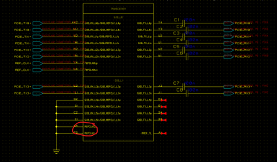
I have shown you the screenshot before but can I use REFCLK1 as an alternative PCIe clk? REF_CLK comes on to our board through a backplane from the Root Complex. If we have signal integrity issues then I'd like to connect a local 100Mhz LVDS clock to REFCLK1. Will this work?
Thanks
Frank
- Mark as New
- Bookmark
- Subscribe
- Mute
- Subscribe to RSS Feed
- Permalink
- Report Inappropriate Content
Hi,
If you are using the bottom Transceiver then you can only use REFCLK0.
- Mark as New
- Bookmark
- Subscribe
- Mute
- Subscribe to RSS Feed
- Permalink
- Report Inappropriate Content
- Mark as New
- Bookmark
- Subscribe
- Mute
- Subscribe to RSS Feed
- Permalink
- Report Inappropriate Content
- Mark as New
- Bookmark
- Subscribe
- Mute
- Subscribe to RSS Feed
- Permalink
- Report Inappropriate Content
Hi @JohnT_Intel sorry I replied to the wrong post. I have a new case open. 05408528. Can you respond to this please?
Thanks
Frank
- Subscribe to RSS Feed
- Mark Topic as New
- Mark Topic as Read
- Float this Topic for Current User
- Bookmark
- Subscribe
- Printer Friendly Page


