- Mark as New
- Bookmark
- Subscribe
- Mute
- Subscribe to RSS Feed
- Permalink
- Report Inappropriate Content
Hi,
I've been analyzing the Altera PCIe Hard-IP cores. I started off with the Qsys PCIe code, since it had the simplest interface. Here's the test setup: * Quartus 11.0, 11.1sp1, 11.1sp2 * Cyclone IV GX Transceiver Starter Kit - x1 PCIe end-point with 125Mhz application clock - x1 PCIe end-point with 62.5MHz application clock * Stratix IV GX Development Kit - x8 PCIe end-point with 250Mhz application clock - x4 PCIe end-point with 125Mhz application clock The Qsys designs are similar to the example provided in the PCIe Compiler Users Guide. I've described the design process and have written automated synthesis scripts (making it easy for anyone to reproduce my results): http://www.ovro.caltech.edu/~dwh/correlator/pdf/altera_pcie_analysis.pdf (http://www.ovro.caltech.edu/%7edwh/correlator/pdf/altera_pcie_analysis.pdf) http://www.ovro.caltech.edu/~dwh/correlator/pdf/altera_pcie.zip (http://www.ovro.caltech.edu/%7edwh/correlator/pdf/altera_pcie.zip) The Cyclone IV GX designs were failing timing due to the multi-corner timing optimization setting defaulting to off. The designs pass timing for a -6 speed grade device, but fail for -7 speed grade. This is inconsistent with the PCIe Compiler Users Guide. The Stratix IV GX x8 design still fails timing analysis (ever so slightly). I'm in the process of trying to resolve this via an Altera Service Request. The x4 design has a problem with width negotiation; its sometimes x4, but often x1 or x2, I'm not sure what is wrong. If anyone wants to try these designs, or has any insight or suggestions on where I may have gone wrong, I'd love to know, thanks! Cheers, DaveLink Copied
22 Replies
- Mark as New
- Bookmark
- Subscribe
- Mute
- Subscribe to RSS Feed
- Permalink
- Report Inappropriate Content
Dave,
Where is this failing timing? I am currently 'debugging' a design that is.. Quartus 11.0 (I can't run the Qsys system through 11.1, even if I regenerate the Qsys system in 11.1 [which I can do without error]). Custom board Cyclone IV x1 Hard IP PCIe end-point with 125Mhz application clock Simple memory mapped interface to custom logic. This is failing on core-clock -> core clock transfers internal to the hard IP according to Timequest. As far as I can see everything's constrained properly. [Edit] I forgot to say the board's been built with '7 devices, the PCIe spec says the core should work on '8s.[/Edit] I've been meaning to raise a SR for about a week but if you could get it sorted out that would be very helpful. :) Nial- Mark as New
- Bookmark
- Subscribe
- Mute
- Subscribe to RSS Feed
- Permalink
- Report Inappropriate Content
From a quick ckeck of your document I think my design's failing in a similar way.
I see you also have a review of Altera's example designs..... I got a design from the Altera wiki "c4gx_qsys_pcie_gen1x1". This is verilog based, my background is VHDL. It took me a long time to realse that at the top level the altgx_reconfig module is connected to the core with undeclared signals (reconfig_fromgxb and reconfig_togxb) which in Verilog are treated as a single bit, so it's effectively not connected . The design works but it's incredibly bad for Altera to be releasing this as an 'example'. I've complained about this elsewhere on this forum so it might be fixed but it's worth keeping an eye out for. Nial- Mark as New
- Bookmark
- Subscribe
- Mute
- Subscribe to RSS Feed
- Permalink
- Report Inappropriate Content
Hi Nial,
Thanks for the feedback! I have been very unimpressed with the Altera examples, and the hundreds of disconnected nets that their examples and IP cores generate. It makes it very difficult to spot real errors. All of these warnings could be suppressed with the correct use of generics/parameters and synthesis directives. I did file an SR and I talked to the engineers at Terasic. The guys at Terasic suggested making sure the fitter setting OPTIMIZE_MULTI_CORNER_TIMING was ON. That cleared the errors on the Cyclone IV GX designs, but made no change in the fitter results for the Stratix IV GX designs. I received a response from Altera and it included a couple of example designs. I'll check them out and post an update. Cheers, Dave- Mark as New
- Bookmark
- Subscribe
- Mute
- Subscribe to RSS Feed
- Permalink
- Report Inappropriate Content
Hi all,
I've updated the text of the original post above, since I removed the build files (since the design has changed slightly). The design changes were; 1) Turn on multi-corner timing optimization. 2) Turn on the reconfiguration reset input and drive it with a signal derived from the PLL locked output The Cyclone IV GX -6 speed grade devices pass timing now, however, -7 does not for the x1 PCIe with 125MHz application clock (it does with 62.5MHz application clock, at least under 11.0). The Stratix IV GX x8 design does not pass timing either. What a pain ... Cheers, Dave- Mark as New
- Bookmark
- Subscribe
- Mute
- Subscribe to RSS Feed
- Permalink
- Report Inappropriate Content
Thanks for your examples and instructions! This is very useful for understanding of Altera's tools.
One more bit of information to consider: we use Altera's dev. board with Stratix IV and used their PCIe+DDR3 example as a starting point. It turns out that when their example is synthesized and P&R'ed, it does not meet timing and the README file says to ignore it! And it actually works on the board! So, the question is if Altera tools say that timing requirements are not met, does it really mean the timing requirements are not met? Conversely, if Altera tools say that timing requirements are met, does it really mean the timing requirements are met? Not a lot of confidence.- Mark as New
- Bookmark
- Subscribe
- Mute
- Subscribe to RSS Feed
- Permalink
- Report Inappropriate Content
--- Quote Start --- One more bit of information to consider: we use Altera's dev. board with Stratix IV and used their PCIe+DDR3 example as a starting point. It turns out that when their example is synthesized and P&R'ed, it does not meet timing and the README file says to ignore it! And it actually works on the board! --- Quote End --- That was part of my initial frustration - none of the example designs appeared to meet timing! The fact that it works on the board is not too surprising, if you look at the failure paths. Often the failures occur at process extremes, so there's a good chance that you are just 'lucky' and are not operating near that extreme. The problem is, how can you design a 'robust' system, if the tools complete P&R with timing errors, even after you have told it to perform timing-driven compilation! --- Quote Start --- So, the question is if Altera tools say that timing requirements are not met, does it really mean the timing requirements are not met? --- Quote End --- It means that your design might fail. --- Quote Start --- Conversely, if Altera tools say that timing requirements are met, does it really mean the timing requirements are met? --- Quote End --- Yes, timing requirements are all met, under all process variations (assuming the models are conservative). Cheers, Dave
- Mark as New
- Bookmark
- Subscribe
- Mute
- Subscribe to RSS Feed
- Permalink
- Report Inappropriate Content
My update on this....
As well as not meeting timing I had a problem with an Error 10232 when I tried building a Quartus 11.0 Qsys system in Quartus 11.1sp2. The solution to this was to move a PIO output in the Qsys memory map, this not only cleared the error but from that point on all my designs have been meeting timing. :confused: Nial- Mark as New
- Bookmark
- Subscribe
- Mute
- Subscribe to RSS Feed
- Permalink
- Report Inappropriate Content
Hi Dave,
Did you contact Altera about 'reconfiguration busy' being asserted for ~6ms? Did anyone confirm your timing on another part? Did you determine if a longer reset period before allowing altgx_reconfig to start improves link negotiation for 4x ? Was this support entry posted thanks to your design? www altera com/support/kdb/solutions/rd12172009_309.html Chris- Mark as New
- Bookmark
- Subscribe
- Mute
- Subscribe to RSS Feed
- Permalink
- Report Inappropriate Content
Hi Chris,
--- Quote Start --- Did you contact Altera about 'reconfiguration busy' being asserted for ~6ms? Did anyone confirm your timing on another part? --- Quote End --- I didn't contact Altera about this aspect (my discussions with them were regarding the failure to meet timing). I don't recall if I tested this on multiple parts. --- Quote Start --- Did you determine if a longer reset period before allowing altgx_reconfig to start improves link negotiation for 4x ? --- Quote End --- I didn't try. Have you? --- Quote Start --- Was this support entry posted thanks to your design? www altera com/support/kdb/solutions/rd12172009_309.html --- Quote End --- I don't think so. I do recall seeing recommendations like this, though many of the example designs neglect to implement it. Cheers, Dave- Mark as New
- Bookmark
- Subscribe
- Mute
- Subscribe to RSS Feed
- Permalink
- Report Inappropriate Content
So far I haven't had a problem negotiating at x4 gen2. My design is a custom PCB with different clock sources to the dev board. The reconfig_pll is driven by an external free running clock at 125Mhz on LVDS pins. Also the design passes timing - perhaps this was cleaned up in QuartusII v12. I'm not in a position to measure the reconfiguration time as no chipscope support for my cable.
Chris- Mark as New
- Bookmark
- Subscribe
- Mute
- Subscribe to RSS Feed
- Permalink
- Report Inappropriate Content
--- Quote Start --- So far I haven't had a problem negotiating at x4 gen2. My design is a custom PCB with different clock sources to the dev board. The reconfig_pll is driven by an external free running clock at 125Mhz on LVDS pins. Also the design passes timing - perhaps this was cleaned up in QuartusII v12. --- Quote End --- I'll have to re-run these tests in 12.1 and see if anything has changed. --- Quote Start --- I'm not in a position to measure the reconfiguration time as no chipscope support for my cable. --- Quote End --- Careful, your Xilinx is showing ;) If you have a USB-Blaster cable, then SignalTap should work fine. Cheers, Dave
- Mark as New
- Bookmark
- Subscribe
- Mute
- Subscribe to RSS Feed
- Permalink
- Report Inappropriate Content
--- Quote Start --- I'll have to re-run these tests in 12.1 and see if anything has changed. --- Quote End --- If anything has changed in 12.1?
- Mark as New
- Bookmark
- Subscribe
- Mute
- Subscribe to RSS Feed
- Permalink
- Report Inappropriate Content
--- Quote Start --- I've described the design process and have written automated synthesis scripts (making it easy for anyone to reproduce my results): http://www.ovro.caltech.edu/~dwh/correlator/pdf/altera_pcie_analysis.pdf (http://www.ovro.caltech.edu/%7edwh/correlator/pdf/altera_pcie_analysis.pdf) http://www.ovro.caltech.edu/~dwh/correlator/pdf/altera_pcie.zip (http://www.ovro.caltech.edu/%7edwh/correlator/pdf/altera_pcie.zip) --- Quote End --- Hello, Dave! I would like to reproduce Your PCIe analysis, but on Cyclone IV GX FPGA Development Kit. Please advise - what should be modified in the contents of altera_pcie.zip so that, it could be used with Cyclone IV GX FPGA Development Kit?
- Mark as New
- Bookmark
- Subscribe
- Mute
- Subscribe to RSS Feed
- Permalink
- Report Inappropriate Content
--- Quote Start --- I would like to reproduce Your PCIe analysis, but on Cyclone IV GX FPGA Development Kit. Please advise - what should be modified in the contents of altera_pcie.zip so that, it could be used with Cyclone IV GX FPGA Development Kit? --- Quote End --- Look at the code. Its already split into designs for two boards. It should be fairly easy to figure out how to change it for use on a new board. The main thing you need to change is the top-level pin assignments, i.e., create a template for your kit (I don't have that kit, so haven't created a top-level design for it). You can use the same Qsys systems since they both use on-chip resources. The only difference between the Stratix and Cyclone kits were the number of lanes. I think your kit has x4, so you can copy either the Cyclone starter kit x1 design or the Stratix x4 design, or you can just follow the procedure in the document to create your own Qsys instance, and then look at the existing code to see how to connect it to the top-level template. Cheers, Dave
- Mark as New
- Bookmark
- Subscribe
- Mute
- Subscribe to RSS Feed
- Permalink
- Report Inappropriate Content
--- Quote Start --- My update on this.... As well as not meeting timing I had a problem with an Error 10232 when I tried building a Quartus 11.0 Qsys system in Quartus 11.1sp2. The solution to this was to move a PIO output in the Qsys memory map, this not only cleared the error but from that point on all my designs have been meeting timing. :confused: Nial --- Quote End --- Hi Nial, Could you please explain the statement "move a PIO output in the Qsys memory map", is it specific to your design? I also have the issue of timings fail when using 100MHz clock for gen 1, X1 link in Cyclone IV GX devices. Thanks, laland
- Mark as New
- Bookmark
- Subscribe
- Mute
- Subscribe to RSS Feed
- Permalink
- Report Inappropriate Content
Dave,
I have a situation where I get stale data back to the RC from the ArriaV or Cyclone IV endpoints ... Has to be a logical issue rather than FPGA or Timing. I write to a constant location and read back the same location then compare ... then move on to a new write pattern. It passes until I start the NIOS , even if I just perform a single printf and return. After that I get stale data ... ie the data from the previous iteration of the test ... where the data I get is the data that was written say 8 writes back , sometime more , sometimes less but a constant. I am trying to see in Simulation and setting "Singel DW completer" on. Seen anything like this before ? Thanks, Bob.- Mark as New
- Bookmark
- Subscribe
- Mute
- Subscribe to RSS Feed
- Permalink
- Report Inappropriate Content
Hi Bob,
--- Quote Start --- I have a situation where I get stale data back to the RC from the ArriaV or Cyclone IV endpoints ... Has to be a logical issue rather than FPGA or Timing. I write to a constant location and read back the same location then compare ... then move on to a new write pattern. It passes until I start the NIOS , even if I just perform a single printf and return. After that I get stale data ... ie the data from the previous iteration of the test ... where the data I get is the data that was written say 8 writes back , sometime more , sometimes less but a constant. I am trying to see in Simulation and setting "Single DW completer" on. --- Quote End --- My first question would be can you reproduce this in simulation; I guess "I am trying to see ... " means you have not yet reproduced it. How about SignalTap II tracing of the o --- Quote Start --- Seen anything like this before ? --- Quote End --- I did not end up using the PCIe core due to its lack of BFMs. This may be different now, but Altera removed the BFMs from Quartus and did not provide any support for PCIe debug/verification, so I changed my design to use a processor with a PCIe end-point (a PowerPC). Cheers, Dave- Mark as New
- Bookmark
- Subscribe
- Mute
- Subscribe to RSS Feed
- Permalink
- Report Inappropriate Content
Ok Dave ..
Yes I am going to run Simulation, but it is difficult to get the NIOS II stimulation ... since as I understand that , it is just a BFM master .. I am thinking that if I can demonstrate using Eclipse, just one NIOS II instrunction being executed under the debugger will cause the conditions to fail, then I may have information that the JTAG debug port is doing something ie enabling the NIOS II data / instruction masters. On SignalTap, that will yield more exact information... I will be able to then say the problem is on the PCIe Hard IP side or on the Avalon MM interconnect fabric. I am currently constraining the PCIe BAR Avalon MM master to be "single DW completer" to see if that will constrain things to issue a single write / read at a time. I am still not sure how to run SignalTap and Eclipse at the same time since Eclipse is using the JTAG / USB port that SignalTap would use. It seems like I would need to commit the NIOS II SW + bootloader to Flash so Quartus would be in control of the JTAG Ok on PowerP ... I was in PowerPC land for some time.- Mark as New
- Bookmark
- Subscribe
- Mute
- Subscribe to RSS Feed
- Permalink
- Report Inappropriate Content
Hi Bob,
--- Quote Start --- Yes I am going to run Simulation, but it is difficult to get the NIOS II stimulation ... since as I understand that , it is just a BFM master .. --- Quote End --- The NIOS II is an Avalon-MM master. What will likely make your "simulation" experience more useful is to ignore the NIOS II and add a Avalon-MM BFM Master. You would then create a testbench with Avalon-MM master transactions from the BFM that match your NIOS II software instructions that reproduce the issue. Yes, this sounds like double-effort, but the objective here is "debugging", not tool confusion! :) Of course, if its the interaction of the NIOS II processor and PCIe that is causing the "bug" then this sequence may not show the issue. However, that is still a good test, since you will know that the IP should work. You can then add a NIOS II into the mix and just have the NIOS II core perform a loop that triggers the issue, i.e., don't even bother trying to access the NIOS II, just use it as stimulus in your simulation. --- Quote Start --- I am still not sure how to run SignalTap and Eclipse at the same time since Eclipse is using the JTAG / USB port that SignalTap would use. --- Quote End --- Have you just "tried it"? There used to be interaction between the tools that would make things hang (one process waiting for the other), but recently things appear to have gotten better. If you're working from Windows, you could also try Linux (which uses a different driver interface to the USB-Blaster). Cheers, Dave- Mark as New
- Bookmark
- Subscribe
- Mute
- Subscribe to RSS Feed
- Permalink
- Report Inappropriate Content
Ok Thanks Dave,
I understand ... believe it or not, after some thought experiment on the weekend ... I figured I would force "Single DW completer" for the PCIe Hard IP and now my test to park on a IMEM location and write and read back patterns immediately works even after NIOS is running. See image below . This tells me that the PCIe Hard IP master may have been doing something wierd. And the NIOS II running maybe changed the state of how the Avalon MM interconnect was behaving such that the PCIe Avalon MM master , BAR1, was getting stale data back on reads. I may still try simulating with the "Single DW completer" not checked to see what the BAR1 master is doing. I am interested in your note about the PCIe simulation support. I have dug into the sample testbench that is generated... The RC memory write/read/compare test needs to be made more general since the BFM assembles a Write transaction, writes the address to that location ... I would like a more general call that writes data as a parameter to a random address. So, I will move on and next need to commit NIOS II SW to FLASH which is where I had problems previously. Then CVP and NIOS II SW load via the PCIe link. Best Regards, Bob.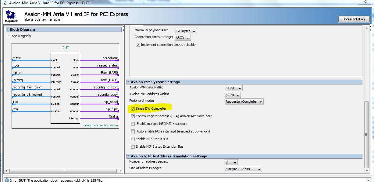
Reply
Topic Options
- Subscribe to RSS Feed
- Mark Topic as New
- Mark Topic as Read
- Float this Topic for Current User
- Bookmark
- Subscribe
- Printer Friendly Page