- Mark as New
- Bookmark
- Subscribe
- Mute
- Subscribe to RSS Feed
- Permalink
- Report Inappropriate Content
Hi,
In the CycloneV GX project, I configured the SDI II core as follows:
bidir, 3G SDI only, transceiver and protocol, CMU, dynamic switching off.
I found out that the SDI output in my project is always synchronous with a frequency of 148.5 Mhz from the dedicated REFCLK pin of the transceiver port. This frequency is connected to megafunctions via xcvr_refclk.
If I try to output the 3G-SDI stream from the color bars generator from the example (sdi_ii_sync_gen) based on the frequency xcvr_refclk = 148.5 Mhz (transceiver REFCLK input), then the image is normal.
On my board, I have a jitter-cleaner chip, which from the horizontal synchronization of the input signal makes a clean frequency of 148.5 MHz (let's call it ExtClear_pclk). Frequency in the allowable range, stable.
If I launch the sdi_ii_sync_gen generator at this frequency, then horizontal interference (stripes, signal disruption) appear in the active video with a certain periodicity.
A similar situation is obtained if I use the sdi_ii_ed_loopback block from the example. This block transmits a parallel stream of 20-bit from the input port to the output. When analyzing SDI from megafunction serial output, I see an input with horizontal stripes.
When capturing video with stripes, I see that samples are being skipped from the input stream. I concluded that my output stream is always synchronous to the fixed frequency xcvr_refclk.
tx_pclk - Transmitter core parallel clock signal. This clock signal must be drivenby the by parallel output clock from TX transceiver tx_clkout.
tx_clkout - in my case xcvr_refclk is always synchronized.
So the parallel stream must be synchronous to xcvr_refclk.
1) How to output the SDI stream on a different reference frequency?
How do I the SDI stream pass through the board, because the input stream is always non-synchronous xcvr_refclk?
Below you can find the file in which I connect the input stream to the output.
How to connect the signals so that the stream is synchronized ExtClear_pclk?
2) If I use one 3G-SDI signal standard (1080p50, 1080p60), do I need a reconfiguration unit?
Best regards, Aleksander
UPD: Problems in video from SDI II core: https://yadi.sk/i/Zc6LRt-k92BheA
- Tags:
- Programmable Devices
Link Copied
- Mark as New
- Bookmark
- Subscribe
- Mute
- Subscribe to RSS Feed
- Permalink
- Report Inappropriate Content
Hi,
- Just to clarify. Do you mean that if you connect the tx_coreclk to ExtClear_pclk, then the problem appears? As per the user guide, the tx_coreclk must be always stable and it can share with xcvr_refclk. If the ExtClear_plck is a clean & stable clock, why not it used as refclk for SDI TX if this is coming from the transceiver dedicated clock pin? Are you implement SDI loopback as SDI RX -> FIFO -> SDI TX? If yes, probably the example in alterawiki is helpful to you. https://fpgawiki.intel.com/wiki/Triple-rate_SDI_II_Reference_Design_for_Stratix_V,_Arria_V_%26_Cyclone_V_devices
- You do not need to perform TX clock switching but the SDI II IP is still required to connect to the reconfiguration controller.
Regards -SK
- Mark as New
- Bookmark
- Subscribe
- Mute
- Subscribe to RSS Feed
- Permalink
- Report Inappropriate Content
Hi Lim,
Thanks for your reply and help!
>Do you mean that if you connect the tx_coreclk to ExtClear_pclk, then the problem appears?
Yes. 3GSDI bitrate is (20*148.5) = 2970 Mbit/s. As far as I understand from the test results, the output bit rate on my board from transceivers is always (xcvr_refclk*20)Mbit/s. xcvr_refclk - from dedicated transceivers REFCLK pins. How do I need to connect the signals so that the bitrate is (ExtClear_pclk*20)Mbit/s?
>If the ExtClear_plck is a clean & stable clock, why not it used as refclk for SDI TX if this is coming from the transceiver dedicated clock pin?
The problem is that in one bank of transceivers I have two asynchronous SDI channels. In one FPGA there are two such banks (four SDI IO channels). There are really four ExtClear_pclk signals: ExtClear_pclk[3:0]. The task of the board is to check and pass through the input streams. All SDI channels are non-synchronous. Therefore, I need to make sure that the bitrate of each channel is (ExtClear_pclk[i]*20), where i=0..3 - is the channel number. Now all ExtClear_pclk[3:0] signals are connected via dedicated clocks inputs. These ExtClear_pclk[3:0] signals are synchronous to the bitrate of the corresponding SDI inputs, but without input jitter.
>Are you implement SDI loopback as SDI RX -> FIFO -> SDI TX?
Yes. SDI[i] RX port -> FIFO[i] (sdi_ii_ed_loopback) -> SDI[i] TX port, where i=0..3 - is the channel number.
>probably the example in alterawiki is helpful to you
I saw this page, but unfortunately links to projects on this pages do not work after the transfer to the Intel site. Where can I download the file C5gtsdi ii top.zip?
>You do not need to perform TX clock switching but the SDI II IP is still required to connect to the reconfiguration controller.
That is, the initial setup of the transceiver is still performed, even if the video standard does not change during operation?
Best regards, Aleksander
- Mark as New
- Bookmark
- Subscribe
- Mute
- Subscribe to RSS Feed
- Permalink
- Report Inappropriate Content
Hi Aleksander,
I attached the example from wiki for your reference.
If your design is doing SDI RX -> FIFO - SDI TX, then you need a external VCXO to sync the clock so that the FIFO won't over flow or underflow. Could you please check if the FIFO is overflow or underflow in your case? The output of the VCXO should connect to the TX refclk, and the txcoreclk is suggested to share with TX refclk. Please look at the following document for the implementation of VCXO in other examples.
https://www.intel.com/content/dam/www/programmable/us/en/pdfs/literature/an/an668.pdf
https://www.intel.com/content/dam/www/programmable/us/en/pdfs/literature/ug/ug-sdi-ii-de.pdf
Regards -SK
- Mark as New
- Bookmark
- Subscribe
- Mute
- Subscribe to RSS Feed
- Permalink
- Report Inappropriate Content
Hi SK Lim,
There is a VCXO on my board. I connected this frequency (148.5Mhz) to the REFCLK and sample SDI RX -> FIFO - SDI TX works. Thank!
There was another question.
The TX PLL captured CMU PLL. But CMU PLL is alone in the transceiver bank (Cyclone V GX). So, can I place only one duplex 3G-SDI channel in one transceiver bank if other banks are busy? Can I put only two duplex asynchronous SDI channels in two transceiver banks of chip?
Is it possible to implement TX PLL using fPLL or channel PLL in this FPGA family?
Are there any estimates (or rules) for the maximum number of SDI channels for Cyclone 10 GX family?
Best regards, Aleksander
- Mark as New
- Bookmark
- Subscribe
- Mute
- Subscribe to RSS Feed
- Permalink
- Report Inappropriate Content
Each Transceiver bank has 6 channels with two CMU PLLs that you can use for the duplex SDI loopback. You are fine to implement two duplex channel in a single or two transceiver banks. FPLL is not supported for SDI II in Cyclone V device. If the TX channels can share the same CMU PLL (no dependency on RX), which mean each transceiver bank can implement maximum 6 SDI TX and 5 SDI RX.
Regards -SK
- Mark as New
- Bookmark
- Subscribe
- Mute
- Subscribe to RSS Feed
- Permalink
- Report Inappropriate Content
Hi SK Lim,
>Each Transceiver bank has 6 channels with two CMU PLLs that you can use for the duplex SDI loopback.
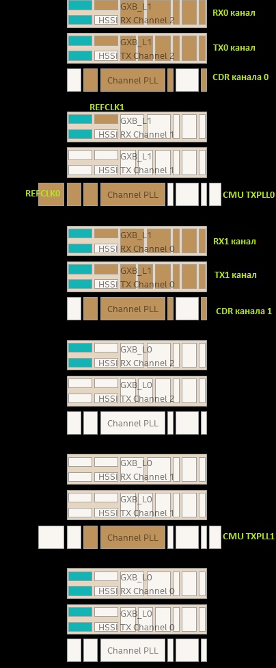
I wanted to clarify: there are two CMUs in each bank or in the whole chip? Chip is 5CGXFC4C6F23. I placed in the project two channels SDI loopback. Below is a screenshot from the Chip Planner ("канал"="channel"). The third channel does not fit, as there is not enough space for the location of the third channel cmu_pll.tx_pll.
Thanks for your help.
Best regards, Aleksander
- Mark as New
- Bookmark
- Subscribe
- Mute
- Subscribe to RSS Feed
- Permalink
- Report Inappropriate Content
Yes, you are right. Each Transceiver bank in Stratix V device has 6 channels (2 CMU PLL), but for cyclone V, each transceiver bank has 3 channels (1 CMU PLL).
Regards -SK
- Subscribe to RSS Feed
- Mark Topic as New
- Mark Topic as Read
- Float this Topic for Current User
- Bookmark
- Subscribe
- Printer Friendly Page