- Mark as New
- Bookmark
- Subscribe
- Mute
- Subscribe to RSS Feed
- Permalink
- Report Inappropriate Content
I wanted to know if anyone has used the Altera Stratix4GX PCIe card as
a root port. I have used it as endpoint but have not used as a root- port. As an endpoint all I have to do is plug in the card to a motherboard. But as a root-port, it needs to send out the requests to end point.Link Copied
- Mark as New
- Bookmark
- Subscribe
- Mute
- Subscribe to RSS Feed
- Permalink
- Report Inappropriate Content
So you have to build your own motherboard or use a eval card that has a PCIe socket to let another PCIe card connect to your root port.
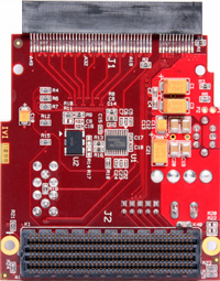
E.g., look at that board: altera stratix iv gx/gt pci express gen 2 / usb 3.0 / sfp+ development platform (http://www.hitechglobal.com/boards/stratix4gx.htm) from hitech global (http://www.hitechglobal.com). http://www.hitechglobal.com/images/S4GX-PCIE.jpg It has a general-purpose connector on top which allows for adapters to be used. One of these is a PCIe plug adapter called »FMC daughter card with x8 PCI Express Root«: http://www.hitechglobal.com/images/PCIExpress_FMC_f.jpg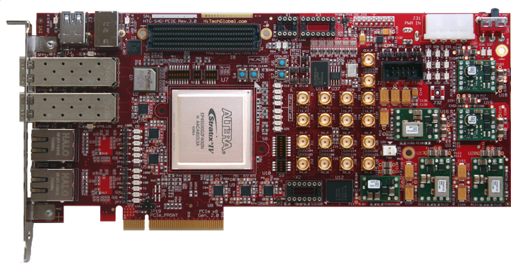
- Mark as New
- Bookmark
- Subscribe
- Mute
- Subscribe to RSS Feed
- Permalink
- Report Inappropriate Content
Thanks for getting back to me. In my application, I want to use the Altera Stratix4GX as the main rootport. I would like to feed the TLPs to it using Avalon Streaming interface which then is sent out to all other PCIe devices on the motherboard.
So in my application, the block diagram will look like as below: Processor --> Altera Stratix4gx root port --> Root port on the motherboard --> Reset of the devices on the motherboard. I notice that the Altera Stratic4gx root port has Base address register, That filters out only specific requests (?) In my application I need the ability to send out any cycles from processor to the root port on the motherboard via the Stratix4GX Root port. Is that possible? I am bit confused about having BAR in root port which limits this? Thanks for prompt response.- Mark as New
- Bookmark
- Subscribe
- Mute
- Subscribe to RSS Feed
- Permalink
- Report Inappropriate Content
I would be surprised if you can put a root port on a PCIe expansion card handled by a root port on the motherboard, so the answer is: No, it’s not possible.
As written, the only way to make use of a root port in an FPGA is to drive another end point, or a switch with multiple end points behind it, when connected properly using such a dev kit with a PCIe socket card. Or you can build your own motherboard. edit: Maybe you meant something different? You don’t have to be a root port to send out requests on PCIe, but you have to have OS driver support to have proper I/O to I/O communication between your device and another end point. Most of the time it’s easier to let the devices communicate just with the main processor behind the motherboard root complex which then orchestrates data transfers using OS drivers. Only very high I/O rates or low-latency applications require direct device-to-device communication.- Mark as New
- Bookmark
- Subscribe
- Mute
- Subscribe to RSS Feed
- Permalink
- Report Inappropriate Content
--- Quote Start --- I notice that the Altera Stratic4gx root port has Base address register, That filters out only specific requests (?) In my application I need the ability to send out any cycles from processor to the root port on the motherboard via the Stratix4GX Root port. Is that possible? I am bit confused about having BAR in root port which limits this? --- Quote End --- I am pretty sure that the root port can send out any requests, but you may have to make use of the most native PCIe application interface like the Avalon ST where you issue all the TLPs natively, instead of an SOPC design. I’m just developing an end point design with AST interface. I have heard not the best critics about the SOPC adaptors supplied by Altera, so I wanted to make my mistakes myself. I don’t know precisely which BAR decoding you refer to, but I don’t think it’s related to what requests can go out to the PCIe bus/link.
- Mark as New
- Bookmark
- Subscribe
- Mute
- Subscribe to RSS Feed
- Permalink
- Report Inappropriate Content
--- Quote Start --- I would be surprised if you can put a root port on a PCIe expansion card handled by a root port on the motherboard, so the answer is: No, it’s not possible. As written, the only way to make use of a root port in an FPGA is to drive another end point, or a switch with multiple end points behind it, when connected properly using such a dev kit with a PCIe socket card. Or you can build your own motherboard. edit: Maybe you meant something different? You don’t have to be a root port to send out requests on PCIe, but you have to have OS driver support to have proper I/O to I/O communication between your device and another end point. Most of the time it’s easier to let the devices communicate just with the main processor behind the motherboard root complex which then orchestrates data transfers using OS drivers. Only very high I/O rates or low-latency applications require direct device-to-device communication. --- Quote End --- I am not yet clear on why we can not have the following topology if Altera Stratix4GX is truely a root-port. I understand that one may need a logic to convert the processor cycles into Avalon Streaming interface cycles. But that may not be too bad. Processor --> Stratix4GX Root Port --> Root on Motherboard (Chipset) --> Reste of the Motherboard devices. I am hoping that in above configuration, the Stratix4GX can pass any requests/completions from processor to Chipset and from chipset to the processor. When I generated the root port design using megawaizrd flow, it asked about adding BAR in the root port. It seems that the root port allows some memory mapped I/O for itself if this is required but in my application I just need to pass the requests/completions back and forth beween the processor and chipset. I am not sure why is that not possible.
- Mark as New
- Bookmark
- Subscribe
- Mute
- Subscribe to RSS Feed
- Permalink
- Report Inappropriate Content
You cannot connect your root port in the Stratix4GX with the root port on the motherboard. There must be only/exactly one root complex in the PCIe fabric, just like in PCI where you can also have just one root complex that drives DEVSEL#, etc. Please refer to PCIe Spec Section 1.3 »PCI Express Fabric Topology«.
Again, it’s not possible the way you want it. You can only drive your own, separate PCIe link as a root port as described above: Design a motherboard with your Stratix4GX as the root port, and it will work. But I’m still not convinced that a root port is what you really want to instantiate. As an endpoint in a PCIe slot, you can act as a bus master and issue DMA transfers on your own, issued by your CPU. But you cannot be another root port. Period. I cannot help you for the BAR question as I am not into root port design.- Mark as New
- Bookmark
- Subscribe
- Mute
- Subscribe to RSS Feed
- Permalink
- Report Inappropriate Content
--- Quote Start --- You cannot connect your root port in the Stratix4GX with the root port on the motherboard. There must be only/exactly one root complex in the PCIe fabric, just like in PCI where you can also have just one root complex that drives DEVSEL#, etc. Please refer to PCIe Spec Section 1.3 »PCI Express Fabric Topology«. Again, it’s not possible the way you want it. You can only drive your own, separate PCIe link as a root port as described above: Design a motherboard with your Stratix4GX as the root port, and it will work. But I’m still not convinced that a root port is what you really want to instantiate. As an endpoint in a PCIe slot, you can act as a bus master and issue DMA transfers on your own, issued by your CPU. But you cannot be another root port. Period. I cannot help you for the BAR question as I am not into root port design. --- Quote End --- From your feedback, I get the impression that the FPGA endpoint can handle this. But I am not sure. In this scenerio, can the FPGA endpoint start talking to the root-port chipset on power-up (or cold reset)? There may be low level handshake between the root port chipset and the FPGA endpoint - on power up but I am not sure if that enables the FPGA endpoint to start talking like a real processor to the root-port chipset. Basically the PCIe link between the FPGA end-point and the root-port needs to be primary bus. I am not sure if this is possible.
- Mark as New
- Bookmark
- Subscribe
- Mute
- Subscribe to RSS Feed
- Permalink
- Report Inappropriate Content
You can’t not use the main processor on the mainboard. You can’t re-route the the root port activity to a processor behind a PCIe link. All PCIe activity is initiated by the operating system on the CPU behind the root complex, and that’s only the main CPU on the base board.
If you really want/need to have a custom processor act as the PCIe root device, you have to build your own motherboard. Especially, if you want to use a standard COTS chipset you have to mimic the matching CPU local bus (or HyperTransport, etc.), but then you don’t need the PCIe root port in the FPGA in the first place. PCIe is strictly top–down. On top there is the root port, below are end points and switches. No way you can “reverse polarity” on a link and let an end point act as a super-root complex, disabling the main CPU.- Mark as New
- Bookmark
- Subscribe
- Mute
- Subscribe to RSS Feed
- Permalink
- Report Inappropriate Content
In that case, how does the PCIe speedbridge work? The PCIe speedbridge connects the processor to a chipset rootport. This device is completely transaparent to the OS and driver. It must be all custom and does not really leverage the hard IP?
- Mark as New
- Bookmark
- Subscribe
- Mute
- Subscribe to RSS Feed
- Permalink
- Report Inappropriate Content
Haven’t heard of speedbridge yet. Interesting stuff. here are the docs (http://www.cadence.com/rl/resources/datasheets/sb_express_ds.pdf).
I think you misinterpret its function, though. The device can emulate two different things: (a) a PCIe end point, transparently visible to the PC the speedbridge is plugged into. (b) a PCIe root port when connected to a nice little board (the one with the blue-colored frame) with two sockets, probably connected 1:1, where the second plug is for a PCIe adapter card (e.g. SATA, USB3, 10G Ethernet) you want to test your root port against. The docs don’t speak – not even suggest – that the speedbridge can act as a root port, connected to a PC’s chipset root port. The specified transparency relates to the use of the drivers running on the PC running the speedbridge card in endpoint mode, emulating the real device function.- Mark as New
- Bookmark
- Subscribe
- Mute
- Subscribe to RSS Feed
- Permalink
- Report Inappropriate Content
In first mode PCIe endpoint mode, I would like to to use the Avalon Streaming interface as a connection to my processor. It seems that in order to do the endpoint emulatin , the speedbridge has to have complete control over the motherboard - including PCI configuration of all devices. The PCIe side of the FPGA connects to the chipset root port on the PC (this technically may be the secondary PCIe link). My processor will send out all the PCIe config cycle over the Avalon streaming interface to configure the motherboard devices. I am not sure if this is possible using the FPGA hard IP. Can the FPGA endpoint pass all the transaction generated on Avalon Streaming TX interface without claiming them? Allso can the root-port chipset support this mode of communication?
- Mark as New
- Bookmark
- Subscribe
- Mute
- Subscribe to RSS Feed
- Permalink
- Report Inappropriate Content
If I just have a southbridge (not a root port) on the motherboard then it seems that I can use the FPGA in root port mode. I am not sure what happens to the root-port inside the processor that is connected to the strteaming interface
- Mark as New
- Bookmark
- Subscribe
- Mute
- Subscribe to RSS Feed
- Permalink
- Report Inappropriate Content
Reply to# 12: No, in order to emulate a PCIe end point (as layed out by me as option (a)), a speedbridge just has to behave like an end point, and it does so without being a root port. It cannot act as the root port when plugged into a PC. Regarding your final two questions: The FPGA endpoint should pass all transactions generated in your application, sent over AST TX. No, the root port chipset won’t support that kind of another root port configuring the PCIe fabric, this is the task of the processor behind the one and only root complex. In order to be the root port, you have to build a structure like documented in Section 1.3 of the PCIe spec, with your FPGA on top – not as a leaf.
Reply to# 13: If you have a southbridge chip that is connected downstream as an end point to the northbridge over PCIe, then you could use an FPGA in root port mode to drive the southbridge. Problem is: You have to connect to the southbridge over the pins that are currently connected to the northbridge/root complex. As you can’t just unsolder the northbridge and put some wires to your FPGA in its place, you have to build a completely new motherboard around your FPGA and southbridge. Otherwise it’s not possible. I have to insist: You cannot make your FPGA a root port, connect it to a COTS motherboard’s PCIe slot and expect your CPU inside/behind the FPGA to mutiny and take over the ship, act as the new root. No way. Nada. These are your options: • Find an FPGA dev board with a PICMG connector (I don’t know whether that actually exists) and make your FPGA a PCIe root port. Then you can take a PCIe backplane and connect multiple COTS PCIe cards to that backplane and let your CPU/FPGA drive them. I have not seen a backplane yet that has a southbridge on it, as most industrial CPU cards with PICMG have them around the CPU, as most southbridge chips are not connected to the northbridge over official PCIe. • Use a PCIe southbridge chip. As I don’t think that there are dev kits available with such a setup, you have to build your own board with your application and the southbridge on it. • Use a COTS northbridge chip. Again, build your own board. Currently there is no chipset that connects to the CPU over PCIe, so you will have to build a different FPGA design that speaks that CPU’s frontside bus language (HyperTransport, QPI, xGTL, etc.). • Write a PCIe end point and let the CPU on the motherboard handle PCIe configuration, drivers etc.- Mark as New
- Bookmark
- Subscribe
- Mute
- Subscribe to RSS Feed
- Permalink
- Report Inappropriate Content
Thanks for taking the time to explain possible solution to this.
For now if we make the following assumptions: (1) Custom designed motherboard with a PCIe slot and only pcie south-bridge and no Northbridge is available. (2) This PCIe slot is used to plug in the FPGA Speedbridge (3) The other side of the PCIe slot is connected to a PCIe southbridge with all the necessary peripherals to boot. Based on your explanation, it seems that I can use the FPGA speedbridge device as a Root port - provided that the the CPU behind avalon Streaming interface does not have integrated root port in it. If yes to the above case then - Can the FPGA speedbridge be completely transparent to the software? From the Avalon Streaming interface back-door when CPU is performing the PCI enumeration, then it is not going to find the FPGA speedbridge as one of the PCI device. As per my understanding, in order to access the config registers inside the FPGA hard IP, one has to use the LMI interface which is not being utilized by the CPU on avalon stream bus. Thus when CPU generates any PCIe config cycles on streaming interface then it will go out in PCIe bus and then to the Southbridge on the motherboard. I can try to run some simulations to get an answer but I thought I ask anyway. Thanks for your help.- Mark as New
- Bookmark
- Subscribe
- Mute
- Subscribe to RSS Feed
- Permalink
- Report Inappropriate Content
I don’t know whether I precisely understand your target architecture.
At first, the architecture you specify in your bullets (1), (2) and (3) looks good, but it’s incomplete. What do you want to use the Speedbridge for? It’s an emulation tool and according to the data sheet it works only in conjunction with the proprietary Incisive Palladium simulation system. It is just thought to help you make a simulated CPU with a PCIe root port drive real PCIe hardware. It is not intended to be a PCIe extender or something similar – that’s what PCIe switches are for. That means, wherever you plug the other side of the Speedbridge into – the Palladium –, this computer cannot use the bridge ‘transparently’ at all, I suspect the simulation platform to be optimized for this simulation task and not for physical transparency. But I am not into Speedbridge/Palladium design, so I can be wrong. So, apart from Speedbridge, let’s say instead of (2) you plug a PCIe FPGA board – maybe a dev kit – into your Custom Mainboard (1). The FPGA is acting as a PCIe root. For argument’s sake, let’s assume that this works physically without mods on the dev kit. Then you put a bridge between your CPU (physical or core) and the AST of the PCIe IP block inside the FPGA. Remember that the PCIe root port is not transparent for your CPU at all, and the bridge will have to maintain all functionality specific to a root complex bridge. That includes and is not limited to CFG space access decoding, Interrupt Message handling from the PCIe leafs, etc. Again, it is impossible from a PCIe architectural standpoint to have any other PCIe root complex between the CPU and the FPGA root port. With proper OS support it might be possible to have multiple PCIe busses with multiple root complexes side-by-side, but I don’t know precisely if that’s possible at all. I think that whatever you intend should be doable with a standard PCIe architecture, so try to stick with that.- Mark as New
- Bookmark
- Subscribe
- Mute
- Subscribe to RSS Feed
- Permalink
- Report Inappropriate Content
Thanks for your feedback. Yes. I would like to use this for CPU simulation. It seems that PCIe FPGA root port hardIP can not be used. May be Cadence custom designed the pass through bridge that accepts the TLPs from Palladium side and converts into PCIe and viceversa. It may not have its own config space. Cadence speedbridge may have added other layers to meet the PCie spec.
I am not sure if there is a soft IP from FPGA vendor that lets you do similar things.- Mark as New
- Bookmark
- Subscribe
- Mute
- Subscribe to RSS Feed
- Permalink
- Report Inappropriate Content
You know, a PCIe root port is not a switch port. If you want to design a PCIe switch, you would have to design a (soft) L2 IP on your own, I think.
In PCIe, a Switch is an addressable and visible entity inside the fabric. It sure does most of its task on L2 which is packet forwarding and maintenance of link-specific DLLP handling like flow control, but it does quite something on L3 as well. A dual-port switch is in fact a bridge, and such a bridge could be designed to be transparent and promiscuous above L2. I think their clever part will be that they don’t emulate the physical layer of the ASIC design but they inject straight into L2 (DLL), that makes them transparent but let the user verify most of his design.- Mark as New
- Bookmark
- Subscribe
- Mute
- Subscribe to RSS Feed
- Permalink
- Report Inappropriate Content
Thanks. I will have to study what it takes to inject the traffic staright into L2 which just one lyaer below Transaction layer. Need to determine output of the Transaction layer and input into the DLL. Is there a soft IP I can use upto DLL?
- Mark as New
- Bookmark
- Subscribe
- Mute
- Subscribe to RSS Feed
- Permalink
- Report Inappropriate Content
I don’t know of any official way to get there.
1) You have to setup the Transceivers to do PCIe L1 (Physical Layer) and supply a proper interface (PIPE). It seems one can use the instantiated pcie_serdes component from the top-level PCIe design from MegaWizard. 2) You have to build your own DLL. That’s what PCIe Spec Chapter 3 is all about. That includes: • Proper handling of L1 at line rate, • link setup, • DLLP handling including power saving stuff, TLP acknowledgement, and flow control according to your buffering capabilities, • proper TLP encapsulation, • error handling (CRC) and retry mechanism, • etc. 3) On top of the DLL you can build whatever interface is appropriate for your setup. 4) remember that while you can rate-adapt in this bridge, you have to maintain all timeouts defined by the PCIe spec, otherwise data gets lost on the lowest level, and that’s not what you want. The following Altera IP functionality should not be in this bridge IP: 1) Configuration space handling, 2) BAR decoding, 3) tag handling, 4) interrupt message generation/decoding, 5) completion timeout, 6) Filtering of unexpected TLPs, 7) etc. Happy Hacking!- Mark as New
- Bookmark
- Subscribe
- Mute
- Subscribe to RSS Feed
- Permalink
- Report Inappropriate Content
Thanks again. What if the processor has the data link layer included in it? In this case the FPGA may need to support is the physical layer supporting Link Training and Flow control.
- Subscribe to RSS Feed
- Mark Topic as New
- Mark Topic as Read
- Float this Topic for Current User
- Bookmark
- Subscribe
- Printer Friendly Page