- Mark as New
- Bookmark
- Subscribe
- Mute
- Subscribe to RSS Feed
- Permalink
- Report Inappropriate Content
I have been developed system which performs simultaneous writing and reading of the same DDR2 RAM (reading from the first half, writing to the second half). Read and write data (32 bit width) are digitally loopbacked while debugging. Memory is 16 bit width, clock rate 150-200 MHz (due to the FPGA limitation). My master controllers are based on Altera examples. They are supported burst mode. System structure is shown in the figure “System1” (it is developed in SOPC Builder).
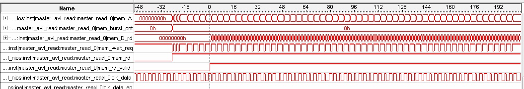
CPU is inactive while read/write operations. It runs usleep() and did not request access to DDR2 RAM. First implementation was system with DDR2-Altmemphy controller (HPC-II) at full rate. Burst count equal to 4 was set everywhere: DDR2 RAM chip, DDR2 Controller local burst, pipeline bridge max burst and my read/write modules. Arbitration shares were about 32-40 for access from my master controllers to pipeline bridge and from bridge to DDR controller. It works fine, System able to simultaneously read and write data in loop with data clock rate about 45 MHz (for 150 MHz controller clock) – it's 0.3 of clock rate. But I was need to decrease clock frequency due to the timing issues. So I set 200 MHz DDR clock and select Half rate mode in DDR2 controller settings (system clock = 100 MHz). Results are shocking. I was ready to get results about 0.3 of system clock, i.e. 30 MHz. And I believed that it can be greater. In the fact I get less than 20 MHz and a lot amounts of wait_request on bus. My following investigation were related with changing burst parameters in various combination (now I set burst count to 8 everywhere). But the results are similar. Figures show SignalTap waveforms. Top half of the figure is read interface and bottom part is write interface. Several signals in the middle (from “data_out” to “clk_data_en”) are data loop back signals. One figure is simultaneous reading/writing and another figure is beginning of read operation. Last things that I made: delete pipeline bridge and connect DDR2 controller system clock to all components (Figure “System2”). Nothing changes. What am I doing wrong? Where is a bottleneck? Also I need to implement the design on platform with 32-bit width DDR2 RAM. So, recommendations from this point of view will be helpful also :) Thank you in advance!- Tags:
- ddr2
Link Copied
- Mark as New
- Bookmark
- Subscribe
- Mute
- Subscribe to RSS Feed
- Permalink
- Report Inappropriate Content
The SOPC automatically generated arbitration between the different memory bus masters is not efficient.
You might want to look into a block called Multi Port Front End: http://www.altera.com/literature/an/an637.pdf This should be able to handle the arbitration in a more efficient way and thus give you more memory throughput. You want each master to be able to issue and complete a burst of data (reads or writes) before switching off to the next mm-master. The larger the burst size, the more throughput to SDRAM you should see.- Mark as New
- Bookmark
- Subscribe
- Mute
- Subscribe to RSS Feed
- Permalink
- Report Inappropriate Content
Hmm. Thanks, it interesting idea. But let's forget about simultaneous multi-mastering access. Second waveform shows reading procedure by one master only. It looks like DDR controller begins new operation when previous is fully completed only. So, it gives delay 16 cycles in each operation. I don't understand reason of the behavior. I always thought that operations are queued in the controller. PS I try the similar design at system with 32-bit RAM and get same results...
- Mark as New
- Bookmark
- Subscribe
- Mute
- Subscribe to RSS Feed
- Permalink
- Report Inappropriate Content
- Subscribe to RSS Feed
- Mark Topic as New
- Mark Topic as Read
- Float this Topic for Current User
- Bookmark
- Subscribe
- Printer Friendly Page