- Mark as New
- Bookmark
- Subscribe
- Mute
- Subscribe to RSS Feed
- Permalink
- Report Inappropriate Content
I'm simulating altsyncram with Modelsim for Cyclone V.
I use altsyncram instantiated as ROM.INCLUDE "altsyncram.inc";
FUNCTION mROM_256x18_1port( clock, address ) returns( q );
PARAMETERS ( FILE_MIF = "FILE.MIF" );
SUBDESIGN mROM_256x18_1port
(
address : INPUT;
clock : INPUT;
q : OUTPUT;
)
VARIABLE
altsyncram_component : altsyncram WITH (
ADDRESS_ACLR_A = "NONE",
CLOCK_ENABLE_INPUT_A = "BYPASS",
CLOCK_ENABLE_OUTPUT_A = "BYPASS",
INIT_FILE = FILE_MIF,
INTENDED_DEVICE_FAMILY = "Cyclone V",
LPM_HINT = "ENABLE_RUNTIME_MOD=NO",
LPM_TYPE = "altsyncram",
NUMWORDS_A = 256,
OPERATION_MODE = "ROM",
OUTDATA_ACLR_A = "NONE",
OUTDATA_REG_A = "UNREGISTERED",
WIDTHAD_A = 8,
WIDTH_A = 18,
WIDTH_BYTEENA_A = 1
);
BEGIN
q = altsyncram_component.q_a;
altsyncram_component.clock0 = clock;
altsyncram_component.address_a = address;
END;
I've create simple project for testing the ROM only. Simple SystemVerilog file to compile parametrized ROM to SystemVerilog netlist to simulate with Modelsim: module ROM_Coeff_AHDL(address,
data_out,
clock
);
input wire address;
output reg data_out;
input wire clock;
mROM_256x18_1port# (
.FILE_MIF ("filt_triangle.mif")
) inst_mROM_256x18_1port
(
.clock (clock),
.address (address),
.q (data_out)
);
endmodule
Testbench. Incrementing address with every clock rising edge: `timescale 1 ps/ 1 ps
module memory_short_tb();
wire address;
wire data_out;
reg clk;
reg addr_counter;
ROM_Coeff_AHDL U_memory(
.address (address),
.data_out (data_out),
.clock (clk)
);
initial begin
clk = 0;
addr_counter = 0;
end
always# 1 clk = ~clk;
always @ (posedge clk) begin
addr_counter++;
end // always
assign address = addr_counter;
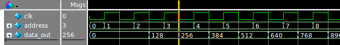
endmodule And the result : http://www.alteraforum.com/forum/attachment.php?attachmentid=12140&stc=1 Data changes on failing edge. But the datasheet https://www.altera.com/content/dam/altera-www/global/en_us/pdfs/literature/ug/ug_ram_rom.pdf says "Rising clock edges" on the page 3-2 . Why data changes on failing edge? Has anybody get the same issue? What is wrong? How to fix issue?
- Tags:
- modelsim
Link Copied
2 Replies
- Mark as New
- Bookmark
- Subscribe
- Mute
- Subscribe to RSS Feed
- Permalink
- Report Inappropriate Content
the DSP Builder Advanced Blockset's Handbook mentioned an example of FFT known as "parallel floating-point fft" and has as a model file "demo_parallel_fpfft.mdl"
and a second one named Variable-Size Floating-Point FFT,[/B] its model file is demo_fpvfft.mdl. Could anyone give me an explanation of what these designs examples demonstrate ?[/B]
- Mark as New
- Bookmark
- Subscribe
- Mute
- Subscribe to RSS Feed
- Permalink
- Report Inappropriate Content
After changing
always# 1 clk = ~clk; to always# 10 clk = ~clk; Data bus updates 1 ps after rising edge of clock.
Reply
Topic Options
- Subscribe to RSS Feed
- Mark Topic as New
- Mark Topic as Read
- Float this Topic for Current User
- Bookmark
- Subscribe
- Printer Friendly Page