- Mark as New
- Bookmark
- Subscribe
- Mute
- Subscribe to RSS Feed
- Permalink
- Report Inappropriate Content
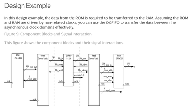
In this example, rom_out, wrreq_o, wrclk are using the same clock trclk.
All above are trigger by rising edge of trclk.
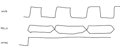
But the fifo write are also refer to rising edge of trclk.
So if there is any small shift, should it cause any risk of timing?
From design point, the fifo data and wrreq should have 180 degree shift related to wrclk.
Does the timing contraint is automatically adjust by quartus itself?
Should we change the wrclk from trclk to ~trclk with 180 degree shift to make the timing to safe area?
- Mark as New
- Bookmark
- Subscribe
- Mute
- Subscribe to RSS Feed
- Permalink
- Report Inappropriate Content
Yes, you can shift the wrclk to 180 degree which can meet timing. There is no saying you can not do that.
Best Regards,
Richard Tan
Link Copied
- Mark as New
- Bookmark
- Subscribe
- Mute
- Subscribe to RSS Feed
- Permalink
- Report Inappropriate Content
Hello,
the design example is based on standard synchronous logic design methods. It expects that all modules operating in a clock domain are clocked by the same clock source and sampling at the same edge. Design implementation and timing analysis guarantee that all register input signals achieve necessary setup and hold times.
You get highest logic speed by clocking all register at the same (usually risng edge). Register hold time is smaller than the "natural" data path delay, if not timing driven synthesis would enforce it.
- Mark as New
- Bookmark
- Subscribe
- Mute
- Subscribe to RSS Feed
- Permalink
- Report Inappropriate Content
I am not how to guarantee the timing to meet it.
It's quite risk as wrreq and fifo_in changes at the rising edge of wrclk.
because rising edge is also used for fifo to push data.
- Mark as New
- Bookmark
- Subscribe
- Mute
- Subscribe to RSS Feed
- Permalink
- Report Inappropriate Content
Most Intel IP has been designed to meet timing. If you worried, you can run the timing analysis stage and the Quartus will analysis and place&route the design as best as possible in order to meet the timing. If there is timing violation, we will see red flag in the timing report.
Best Regards,
Richard Tan
- Mark as New
- Bookmark
- Subscribe
- Mute
- Subscribe to RSS Feed
- Permalink
- Report Inappropriate Content
I believe so, intel IP should be correct. But can you explain a little on it?
Why not move the wrclk to shift 180 degree which may perfectly meet timing constraint?
The clock wrclk rising edge will stay in the middle of fifo_in data.
- Mark as New
- Bookmark
- Subscribe
- Mute
- Subscribe to RSS Feed
- Permalink
- Report Inappropriate Content
0 degree clk gives highest fmax. That's not specfic to FIFO IP, just how synchronous design in FPGA works.
- Mark as New
- Bookmark
- Subscribe
- Mute
- Subscribe to RSS Feed
- Permalink
- Report Inappropriate Content
I appreciate your feedback. Could you tell more about why 0 degree clk gives highest fmax?
- Mark as New
- Bookmark
- Subscribe
- Mute
- Subscribe to RSS Feed
- Permalink
- Report Inappropriate Content
Yes, you can shift the wrclk to 180 degree which can meet timing. There is no saying you can not do that.
Best Regards,
Richard Tan
- Mark as New
- Bookmark
- Subscribe
- Mute
- Subscribe to RSS Feed
- Permalink
- Report Inappropriate Content
Do you need further help in regards to this case?
Best Regards,
Richard Tan
- Mark as New
- Bookmark
- Subscribe
- Mute
- Subscribe to RSS Feed
- Permalink
- Report Inappropriate Content
Do you need further help in regards to this case?
Best Regards,
Richard Tan
- Mark as New
- Bookmark
- Subscribe
- Mute
- Subscribe to RSS Feed
- Permalink
- Report Inappropriate Content
As we do not receive any response from you on the previous question/reply/answer that we have provided. I now transition this thread to community support.
Best Regards,
Richard Tan
p/s: If any answer from the community or Intel Support are helpful, please feel free to give best answer or rate 4/5 survey.
- Subscribe to RSS Feed
- Mark Topic as New
- Mark Topic as Read
- Float this Topic for Current User
- Bookmark
- Subscribe
- Printer Friendly Page

