- Mark as New
- Bookmark
- Subscribe
- Mute
- Subscribe to RSS Feed
- Permalink
- Report Inappropriate Content
Hi there,
I am working on a design uses an ALTGX IP in a Arria II GX device and got the following error in the fitting: Error: Input port CORECLK of GXB Receiver channel PCS "fiber_trx_lev1_aria2gx:Fiber_Lev1_Left|fiber_gx_alt4gxb:U1|receive_pcs0" must be fed by output port CLOCK_OUT of GXB Receiver channel PCS "fiber_trx_lev1_aria2gx:Fiber_Lev1_Left|fiber_gx_alt4gxb:U1|receive_pcs0" because the GXB receiver is not rate-match FIFO enabled or receiver is operating at a dissimilar data rate to the transmitters or receiver can be dynamically reconfigured The attached is a screenshot of the ALTGX configuration structure. The error message seems to suggest me to use the rx_clkout as the rx_coreclk because I didn't enable rate-match FIFO (the other two reason does not apply for my design). Now my questions are: 1. what is the purpose of phase compensation fifo if the input and output has to use the same clock, the rx_clkout (i.e. the recovered clock)? 2. If I have to use the same clock on the two side of the phase compensation fifo, how do I cross the data over to my core clock domain? rate-matching FIFO? 3. If I have to use the rate matching FIFO, is there a configuration that I can still get the recovery clock output (I am using it to sync my local clock)? Any help is appreciated. Hua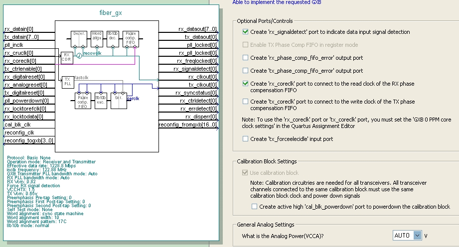
Link Copied
- Mark as New
- Bookmark
- Subscribe
- Mute
- Subscribe to RSS Feed
- Permalink
- Report Inappropriate Content
Hi,
I had almost the same issue as you. You can use a different clock at the output of the fifo, but it has to have exactly the same frequency (which is the case if you use the rx_clkout of gxb1 to feed gxb2). And you have to tell quartus that both clock have the same frequency (GXB_0PPM_CORE_CLOCK property). I was trying for quite a time until I found the correct syntax. Try this: set_instance_assignment -name GXB_0PPM_CORE_CLOCK ON -from "fiber_trx_lev1_aria2gx:Fiber_Lev1_Left|rx_clkout[0]" -to {the serial input port of your top level design[0]} set_instance_assignment -name GXB_0PPM_CORE_CLOCK ON -from "fiber_trx_lev1_aria2gx:Fiber_Lev1_Left|rx_clkout[0]" -to {the serial input port of your top level design[1]} (maybe you need to adapt the command a bit) The strange thing for me is that in the "-to" field you need to assign the serial input port which comes at a much higher rate. But I got it working this way. See http://www.alteraforum.com/forum/showthread.php?t=21970 for my configuration. Cheers.- Mark as New
- Bookmark
- Subscribe
- Mute
- Subscribe to RSS Feed
- Permalink
- Report Inappropriate Content
Hi Chrikell,
Thank you so much for your reply! BTW, how is the quality of the rx_clkout from the gxb. I have the impression that it has lots of jitters and needs to be passed through another pll to attenuate the jitter. Was that the case for you? Cheers, Hua- Mark as New
- Bookmark
- Subscribe
- Mute
- Subscribe to RSS Feed
- Permalink
- Report Inappropriate Content
Hi,
I don't actually know the quality of that signal since I only simulated it so far (the device (Stratix IV GT) we want to use has not yet arrived). I hope it's not too bad since I need the clock for quite some logic ;) But I will surely have a look at that clock. Cheers- Mark as New
- Bookmark
- Subscribe
- Mute
- Subscribe to RSS Feed
- Permalink
- Report Inappropriate Content
Just tried the GXB_0PPM_CORE_CLOCK assignment, it didn't work. :(. Maybe because my source of the core clock is not coming from a gxb directly.
Now, instead of driving the core clock with the recovered clock, is it possible to use a clock of the same frequency from a pll? Does Altera provide this connection? Thanks, Hua- Mark as New
- Bookmark
- Subscribe
- Mute
- Subscribe to RSS Feed
- Permalink
- Report Inappropriate Content
I doubt that this is possible. The rx_clkout is generated using the serial input stream. This depends on the tx_clk of the sending device. A PLL will probably not generate exactly the same frequency (0 PPM difference). This leads to a buffer over- or underflow in the phase-compensating fifo.
You can nevertheless try to change the "-from" field of the command to your non-gxb-clock. Hint: As far as I know, quartus give now feedback if your assignment command point to valid ports or not. Using the assignment editor and in there the node finder can help finding the correct ports/nodes- Mark as New
- Bookmark
- Subscribe
- Mute
- Subscribe to RSS Feed
- Permalink
- Report Inappropriate Content
Tried that too, still doesn't work.
But from the attached screenshot, which is taken from the Arria II GX Device handbook Volume 2 Chapter 2 p.g. 2-18 figure 2-11, the MUX circled in red seems to suggest that Altera does provide the control to choose a clock from the Fabric over the clock from the CDR for the read side of the rx phase compensation fifo. I was going to use a pll in the Fabric to attenuate the jitter in the recovered clock and then fit right back to the phase compensation fifo, so there should be a 0ppm clock difference. Now back to my question 1 in my post 1: 1. what is the purpose of phase compensation fifo if the input and output has to use the same clock, the rx_clkout (i.e. the recovered clock)? I thought the phase compensation fifo is the place where the rx data path crosses clock domain boundary to my core/fabric logic. Am I understanding this wrong? Any comments will be appreciated. Hua
- Mark as New
- Bookmark
- Subscribe
- Mute
- Subscribe to RSS Feed
- Permalink
- Report Inappropriate Content
This Mux is, as far as I'm concerned, to use the rx_clkout of transceiver0 to use as read clock of the fifo of transceiver1 (see attached pic (from Statix IV Handbook Vol 2). (Even though it makes completely sense to use use a pll to recover the clock)
The idea of that is, if I understood it correctly, if you have several transceivers in parallel being used for the same link (as in my case 10 transceivers for one 100G Ethernet link) you can use one of the clocks to drive the logic on the receiver side. The fifo is only there to compensate for phase shifts not to compensate different frequencies. If that would be the case, there would be missing some control signals (such as WrFull or RdEmpty). Have a look at Arria II GX Handbook Vol 2, page 2-54. I used a similar page on the stratix handbook to finally solve my problem. Again a hint: I had some problems rerunning the fitter (start again) without resynthesizing the whole design. It seemed to me as quartus would ignore the assignments in this case.
- Mark as New
- Bookmark
- Subscribe
- Mute
- Subscribe to RSS Feed
- Permalink
- Report Inappropriate Content
--- Quote Start --- If that would be the case, there would be missing some control signals (such as WrFull or RdEmpty). --- Quote End --- Agreed. That's probably why it was called "phase compensation" fifo. I wish some gurus from Altera can confirm this. And if that's the case, I will need another fifo to pass the data path cross clock domain into my core logic. Thanks again. Hua
- Mark as New
- Bookmark
- Subscribe
- Mute
- Subscribe to RSS Feed
- Permalink
- Report Inappropriate Content
Hua,
Some time has gone by since your last reply in this topic and I guess most of your problems have been solved so far. So, I think I won't make you an astonishing revelation if I confirm chrikell's last post regarding the role of phase compensation FIFO: the purpose of this block is only to pass data between two clock domains THAT HAVE THE SAME FREQUENCY. In other words, it's a phase shifter functionnaly similar to x1 PLL. I guess it's simpler for ALTERA chip designers to implement this function with registers issued from a TSMC library Design Kit instead of using PFDs, loop filters, dividers and so on... Moreover if you have to put such a function at every PCS outputs, doing it the "digital way" could save power and add robustness. There is only one detail I can't explain in this FIFO block: the Altera AN573 mentions the phase compensation FIFO may handle 5 UI which I translate (erroneously ?) in "the RX phase comp. FIFO's depth is 5-bit" whereas you would need a single bit (or 2 at most) in the case of same frequency RD/WR signals ? Now, reading back your post#2, I have a question regarding the RX phase comp. FIFO read clock source: you said you had the impression that the rx_clkout from the GXB had a lot of jitter. Therefore my question is "have you probed the "rx_clkout" signal ? If yes, how have you proceeded? If no, how did get this impression?". Indeed, in a Basic/Non-Bonded/10-RX only design, I plan to use a rx_clkout port as common clock driver for the rx_corecll[9..0] inputs but also to clock the entire FPGA fabric. You may easily understand that if I use rx_clkout as a system clock, jitter may be a severe issue... So what level of quality have you experienced with these clocks in your design ? Regards Oliver- Mark as New
- Bookmark
- Subscribe
- Mute
- Subscribe to RSS Feed
- Permalink
- Report Inappropriate Content
Hi Oliver,
We didn't check the quality of the rx_clkout because we decided to use a local clock as our core clock for several reasons besides the jitter concern. And I actually can't remember where I got this jitter concern from, it may be from some talks we had with the local tech support team from Arrow. You might want to check with Altera directly about this, maybe the pll in CDR circuit is good enough to provide the quality you want. Regards, Hua- Subscribe to RSS Feed
- Mark Topic as New
- Mark Topic as Read
- Float this Topic for Current User
- Bookmark
- Subscribe
- Printer Friendly Page