- Mark as New
- Bookmark
- Subscribe
- Mute
- Subscribe to RSS Feed
- Permalink
- Report Inappropriate Content
I have checked the Arria 10 SoC dev kit board, and found the FMC DDR3 interfaces are mismatched connections with A10 SoC back IO.
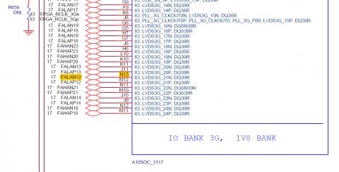
Based on the Device target: 10AS066N3F40E2SGE2. According to the document "Arria 10 SoC Development Kit User Guide", the newest version from website downloading. In page 5-38, for the schematic signal named "FALAN12", it is connected to the FPGA bank "3G", pin number "C4". But according to the board schematic file, in page 28 "FPGA IOs for LVDS links of FMC A Port", the signal "FALAN12" is connected to bank "3G", pin number "N13". So, the pin number shown in user guide is mismatched with the pin number "N13" shown in the schematic. Anyone could help me to check this problem? Thanks.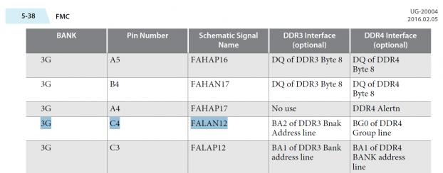
Link Copied
1 Reply
- Mark as New
- Bookmark
- Subscribe
- Mute
- Subscribe to RSS Feed
- Permalink
- Report Inappropriate Content
Reply
Topic Options
- Subscribe to RSS Feed
- Mark Topic as New
- Mark Topic as Read
- Float this Topic for Current User
- Bookmark
- Subscribe
- Printer Friendly Page