- Mark as New
- Bookmark
- Subscribe
- Mute
- Subscribe to RSS Feed
- Permalink
- Report Inappropriate Content
Hi All,
I am trying to build up a system with two NiosII processors, but I am having to figure out how to do the boot job for the two processors. Both of the two processors need to boot from on-chip flash. For the first processor, the .text need to be copied to on-chip RAM from on-chip flash when power-on, while for the second processor, it needs to execute-in-place from the on-chip flash.
I am thinking that I can first let the first processor does the memcpy(copy .text from onchip flash to ram) while hold the soft reset for the second processor. When the first processor is done, when release the soft reset. Then the second processor will jump to the its reset vector address in the flash, and starts executing.
But my question is, after I create the two software applications(one for each processor), how do I merge them together into one .hex file for the flash initialization?
Thank you!
Link Copied
- Mark as New
- Bookmark
- Subscribe
- Mute
- Subscribe to RSS Feed
- Permalink
- Report Inappropriate Content
Hi,
My understanding, Is that your using MAX 10 device, 2-Nios II processor, dual boot and on-chip flash IP.
Processor-1 reset vector to Altera On-chip Flash and exception vector On-chip RAM (Nios II processor application copied from UFM to RAM using boot copier )
Processor-2 reset vector to Altera On-chip Flash and exception vector On-chip Flash(Nios II processor application execute-in place from Altera On-chip Flash (UFM)) is that correct? if yes
UFM data (.HEX file) can be included in either Page_0 or Page_1 only.The Altera On-chip flash does not support two .HEX files for Dual Compressed images configuration mode.
Let me know if my understanding is wrong or if you need any further assistance.
Best Regards,
Anand
- Mark as New
- Bookmark
- Subscribe
- Mute
- Subscribe to RSS Feed
- Permalink
- Report Inappropriate Content
Hi Anand,
Thank you for the reply.
Your understanding is basically right. I am using MAX 10 device, and building a qsys with 2-Nios II processor and boot from on-chip flash. But I don't think I am using Dual Compressed Images configuration mode. I think Dual Boot is for the case when you want to fpga to switch between two designs. For my case I just have one design with two processors running at the same time.
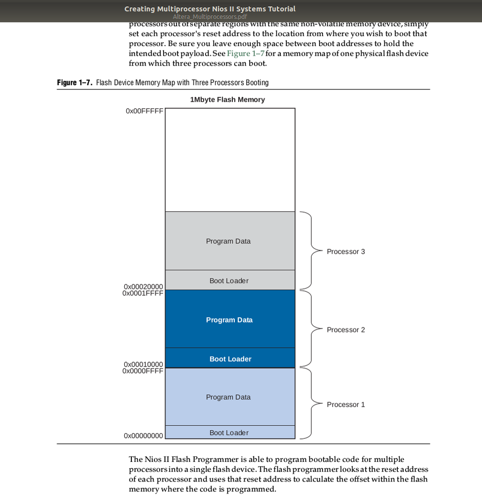
In this document<Creating Multiprocessor Nios II Systems> https://www.intel.com/content/dam/www/programmable/us/en/pdfs/literature/tt/tt_nios2_multiprocessor_tutorial.pdf, it mentions that "The Nios II Flash Programmer is able to program bootable code for multiple processors into a single flash device.". But It does not mention how can I do it, how can I put multiple program codes into one flash device. That's the part that I want to know.
In other word, after build the two software programs for each of the two processors, I got two .elf files(and also two .hex files after make mem_init_generate), how can I merge the files together into one file and then program the flash.
In qsys, I can only specify one .hex file for flash initialization.
- Mark as New
- Bookmark
- Subscribe
- Mute
- Subscribe to RSS Feed
- Permalink
- Report Inappropriate Content
Hi yying5,
Thanks for clarifying.
User Flash Memory (UFM)—to store user data or software applications. Max 10 device supports only one .hex file.
But if you use external flash like qspi you can do it.
Please refer below link for booting methods and steps.
https://www.intel.com/content/dam/www/programmable/us/en/pdfs/literature/an/an741.pdf
Let me know if you need any further assistance.
Best Regards,
Anand
- Subscribe to RSS Feed
- Mark Topic as New
- Mark Topic as Read
- Float this Topic for Current User
- Bookmark
- Subscribe
- Printer Friendly Page
