- Mark as New
- Bookmark
- Subscribe
- Mute
- Subscribe to RSS Feed
- Permalink
- Report Inappropriate Content
Hello,
I have a Max1000 development board and would like to perform a remote system upgrade with it.
I have programmed an SPI interface to send the required data. (Here not necessarily SPI must be used, but I think another interface does not change my problem). Now I want to program the RSU without the Nios.
I have gotten to the point where I need the dual boot ip core to configure the "dual compressed image". An onchip-Ram to store the necessary data and an onchip-Flash to write to the CFM. But here my flash has only an address size of 17 bits, but to rewrite the CFM the address must be at least 18 bits.
Am I missing something here? Is it possible to rewrite the CFM with SPI like this?
Link Copied
- « Previous
- Next »
- Mark as New
- Bookmark
- Subscribe
- Mute
- Subscribe to RSS Feed
- Permalink
- Report Inappropriate Content
First you have to change the FPGA model for project from Settings\Device/Board, and of course redo pin mappings.
Then according to your .rpd file size, you have to change the count value of rsu_data. For example in 10M08, the rpd size is always 143360 bytes. So you can change it for you according to this.
Then in rsu_set you have to change the CFM addresses (onchip_flash_data_address_int) for CFM 0 and 1. (You can check how this addressing calculation done by: https://community.intel.com/t5/FPGA-SoC-And-CPLD-Boards-And/Max1000-Remote-System-Upgrade-via-SPI/m-p/1369068/highlight/true#M22016).
In generics you may be change the CLK_FREQ for UART according to your boards clock.
Maybe some other things should be changed but I don't see them now.
Also you can refer to this: https://community.intel.com/t5/Programmable-Devices/Discrete-RSU-User-Logic/m-p/1385936
and if you check my account you can see similar topics that related to RSU which may help you.
- Mark as New
- Bookmark
- Subscribe
- Mute
- Subscribe to RSS Feed
- Permalink
- Report Inappropriate Content
I found out how to calculate the. rpd file size.
By inspecting the onchip_flash IP in dual mode For 10M08 the Image1 CFM resides between 0x2b000-0x4dfff = 143360 bytes.
This is the size of your .rpd file.
CFM Image 1(called also CFM0) is used as the "factory project", which is the starting project that will hold the manual_rsu design.
The 2 units of CFM Image 2(called CFM1) store together the same amount of memory as CFM Image 1 and are the target for RSU procedure.
As for the UART modules I intend to generate the 115,200X16 = 1.8432Mhz clock by the PLL IP instead the uart_clk_en signal.
Of course that I will need to bridge the clock spaces between the UARTS and the rest of the logic.
As for the ram module I don't understand what is the purpose of this module.
You have mentionted before that it is not required for the RSU activity.
Do you store the incoming stream of data in the RAM to overcome delays in writing to the FLASH(like a large FIFO) or what?
The RAM module, as I mentioned before, blocks most of the memory that is required for signal tap debugging.
If it is not neccessary to the design I will be gratefull if you can instruct me how to get rid of it.
and again, thank you for your time and knowledge.review
- Mark as New
- Bookmark
- Subscribe
- Mute
- Subscribe to RSS Feed
- Permalink
- Report Inappropriate Content
1. You dont need to use a PLL for UART. The UART module in code does it itself. You just need to change the clock frequency which is going to UART module according to your fpga's clock freq.
2. I cut down the ram module and the unnececarry UFM operations from the code. It is now %15 at logic elements and %0 in memory. I'm adding the new project to attachment. But I remembered that before you send the rpd, you have to clear the CFM sector that rpd file is going to write. You can use erase operation from the code (selection 2 in operations) for this purpuse but i dont remember exact number of CFM sectors. UFM-CFMs ranging between 1-5 in total. So you can try it.
- Mark as New
- Bookmark
- Subscribe
- Mute
- Subscribe to RSS Feed
- Permalink
- Report Inappropriate Content
Thank you jozephka99 for the meaningfull work.
A lot of space is free now.
Where in the code I need to make changes due to the type of my device 10M16 instead of yours 10M08?
- Mark as New
- Bookmark
- Subscribe
- Mute
- Subscribe to RSS Feed
- Permalink
- Report Inappropriate Content
As I said first you change the FPGA model from project settings. And then you do the other changes that I mentioned above. Then compile the code so you can see any other missing changes that might broke the compiling. I think you don't need to do lots of changes. You should read the whole code and try to understand it. It is actualy very easy now. And you should read the Intel documentations about the dual boot, on chip flash and rsu. They help you when you stuck in the code.
- Mark as New
- Bookmark
- Subscribe
- Mute
- Subscribe to RSS Feed
- Permalink
- Report Inappropriate Content
From the "MAX 10 user flash memory user guide":
Program Memory in Parallel Mode:
UFM Programming max time = 305uSec
UFM Reset max time = 250 uSec
Tota max time for 4 bytes = 555uSec
for the UART the maximum allowable rate will be = 1/(555uSec/40) =72Kbps
therefore it is advisable to use the rate you have chosen: 57,600 bps in order to avoid losing data.
- Mark as New
- Bookmark
- Subscribe
- Mute
- Subscribe to RSS Feed
- Permalink
- Report Inappropriate Content
Oh, I see now. This explains why am I not successful when I tried 115200 baud rate. Thanks for clearing that out.
- Mark as New
- Bookmark
- Subscribe
- Mute
- Subscribe to RSS Feed
- Permalink
- Report Inappropriate Content
Hi,
In your code of UART module:
constant DIVIDER_VALUE : integer := CLK_FREQ/(16*BAUD_RATE);
This means that for CLK_FREQ = 12.6e6 DIVIDER_VALUE should be = 13.672
Because it is an integer the actual value is 13.
In consequence to this value the accuracy of the uart baude rate is 13.672/13 = 1.0517 or +5.17%.
The problem is that the error is accumulating through the entire transmission and since your state machine starts at the middle of the start bit you have only 50% of the bit width that is allowed to drift. in fact after 8 bits you are accumulating an error of more then 40%, which is still OK but can be risky.
For baud rate of 115,200 DIVIDER_VALUE = 6.8359 and after converted to integer is actually 6 or +13.9% which is, of course a situattion that will not work.
- Mark as New
- Bookmark
- Subscribe
- Mute
- Subscribe to RSS Feed
- Permalink
- Report Inappropriate Content
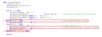
Can you, please, explain in the follwing code of yours the following issues:
1. What should I do to for "write operation needs 3 cycle".
2. "hold nconfig min 250ns, 4 cycle at 12 MHz" isn't that an automatic command and I'm unable to change the number of cycles?
3."elsif(cnt > 60000000) then" has no continuation and also "db_avalon_write" remains at '1' for good?
- Mark as New
- Bookmark
- Subscribe
- Mute
- Subscribe to RSS Feed
- Permalink
- Report Inappropriate Content
First you should know that I gather this timing informations from Intel's configuration user guide (https://www.intel.com/content/www/us/en/docs/programmable/683865/current/fpga-configuration-overview.html) and flash memory user guide (https://www.intel.com/content/www/us/en/docs/programmable/683180/18-0/user-flash-memory-overview.html). You should read them. Your cycle needs will change if your clock is different. After that:
1.Actually you just wait for 3 cycle for "write operation". I did this with using counter. Counter increases every clock cycle. So in 3. cycle it has been waited for 3 cycle = 250ns at 12MHz.
2.As I said you calculate the cycles recpect to your clock cycle. The important thing is the time (250ns) not the cycle count. And it is not an automatic command you drive the bits. If you clear the bits earlier, you may be dont get what you want.
3.Yes it has no continuation because 250ns after the writing the reconfig bits, the device must be restart itself. So I wait here until device restart itself and hold it for 60000000 cycles just for guarantee the operation. So you can change it at least min 250ns.
- Mark as New
- Bookmark
- Subscribe
- Mute
- Subscribe to RSS Feed
- Permalink
- Report Inappropriate Content
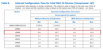
I found in the datasheet the parameter the table of parameters:
I assume that this is the source for the figure 250nS. So, since I'm using 25Mhz CLK I need to change the cnt= 3 to cnt = 7 for db_avalon_write <= '0';
The condition cnt > 60000000 fits to a time of 60,000,000/12.6e6 =4.76 Sec.
The only figure I can find is in the following table:
Do you any insights about this issue?
- Mark as New
- Bookmark
- Subscribe
- Mute
- Subscribe to RSS Feed
- Permalink
- Report Inappropriate Content
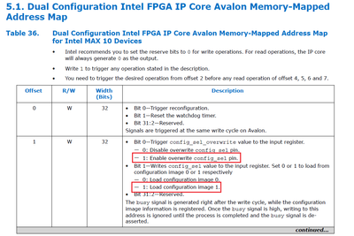
In AN741:
Which complies with the UG-MAX10-Configuration
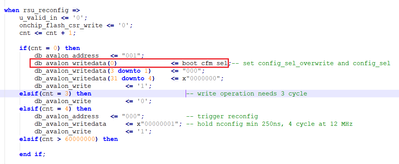
In your code :
The signal boot_cfm_sel should be assigned to writdata(1) and writdata(0) should be set to '1' in order to ignore the physical
config_sel pin and setting the loading image according to boot_cfm_sel.
- Mark as New
- Bookmark
- Subscribe
- Mute
- Subscribe to RSS Feed
- Permalink
- Report Inappropriate Content
Last counter value is not important. It is just waiting for restarting the device. You can change it. And AN741 is not complies with UG-MAX10-Configuration. In AN741 they assign reg 1 to 0x3 that means overwrite selected and Image 1 will be used.
Also sorry, I made a mistake on that code. Here is the revised rsu_reconfig function:
					when rsu_reconfig =>
						u_valid_in <= '0';
						onchip_flash_csr_write <= '0';

						if(cnt = 0) then
							db_avalon_address 	<= "001";
							db_avalon_writedata(0) 					<= '1';										-- set config_sel_overwrite
							db_avalon_writedata(1)					<= boot_cfm_sel;							-- set config_sel
							db_avalon_writedata(31 downto 2) 	<= (others => '0');						-- reserved
							db_avalon_write 		<= '1';
							db_avalon_read 		<= '0';
							cnt <= cnt + 1;
						elsif(cnt = 3) then																			-- write operation needs 3 cycle
							db_avalon_write 		<= '0';
							db_avalon_read 		<= '0';
							cnt <= cnt + 1;
						elsif(cnt = 4) then
							db_avalon_address 	<= "011";														-- busy reg
							db_avalon_read 		<= '1';
							db_avalon_write 		<= '0';
							cnt <= cnt + 1;
						elsif(cnt = 5) then																			-- read operation needs 1 cycle
							db_avalon_read 		<= '0';
							db_avalon_write 		<= '0';
							cnt <= cnt + 1;
						elsif(cnt = 6) then																			-- read data came in 2th cycle
							if(db_avalon_readdata /= x"00000000") then										-- if ufm/cfm busy
								cnt <= 4;																				-- go back until busy flag is over
							else
								cnt <= cnt + 1;
							end if;
						elsif(cnt = 250000000) then																-- high cnt value because of CPU should read the RSU checksum acknowledge
							db_avalon_address 	<= "000";														-- trigger reconfig
							db_avalon_writedata 	<= x"00000001";												-- hold nconfig min 250ns, 4 cycle at 12 MHz
							db_avalon_write 		<= '1';
							db_avalon_read 		<= '0';
							cnt <= cnt + 1;
						else																								-- wait for FPGA trig reconfig
							cnt <= cnt + 1;
						end if;
- Mark as New
- Bookmark
- Subscribe
- Mute
- Subscribe to RSS Feed
- Permalink
- Report Inappropriate Content
Hi jozephka99,
I'm very very interested to learn from your example but I can't download from link.
Can you help me? Maybe you can send your attachment by email?
I'm trying (desperately) to configure my 10m25sa manually by remote, but for me this is a new world, so If you can help me I would be very grateful.
Thank you in advance
Ilaria
- Mark as New
- Bookmark
- Subscribe
- Mute
- Subscribe to RSS Feed
- Permalink
- Report Inappropriate Content
You're exporting everything out of the system, so you're not really building a system. If you make connections in the system without exporting and set proper addressing, the tool checks and makes sure everything in the interconnect is set up correctly and this might fix your issue.
- Mark as New
- Bookmark
- Subscribe
- Mute
- Subscribe to RSS Feed
- Permalink
- Report Inappropriate Content
I want to lead the signals out of the system to be able to set them manually. Just like jozephka99 did in his example. You can use only one nios in the system itself to set them? Or is there another alternative?
- Mark as New
- Bookmark
- Subscribe
- Mute
- Subscribe to RSS Feed
- Permalink
- Report Inappropriate Content
How interesting. The topic is Remote System Upgrade via SPI
However everybody switched to UART... May I make offtopic question and ask about discrete RSU via SPI (or I2C)?
From the very starting point - which IP block should I use for it?


The part I'm using is 10M08 with Verilog. I can translate from VHDL to Verilog, but original Verilog code is preferable.
There is a page with example for RSU via I2C but it does not help. Opening .par file shows only top file for 10M50 used as a I2C host. Structure of the project and used IP blocks are invisible
Besides the description of the project and how to run written for Quartus 16 and for a template it suggests to use an evaluation board that does not exist anymore.
- Subscribe to RSS Feed
- Mark Topic as New
- Mark Topic as Read
- Float this Topic for Current User
- Bookmark
- Subscribe
- Printer Friendly Page
- « Previous
- Next »


