- Mark as New
- Bookmark
- Subscribe
- Mute
- Subscribe to RSS Feed
- Permalink
- Report Inappropriate Content
Hello Everybody. I am an old timer from the Altera Forum. First timer posted on the Intel Forum.
I've been trying to follow the I2C Remote System Upgrade Example (Max 10) for a week now (see attached user guide in pdf). I have bought both the Max 10 Eval kit and Max 10 Development kit as described in the user guide. I followed the instructions to the letter:
- P.g. 11 Programming Master Image into Max 10M50 - Done
- P.g. 11 Programming Slave Image 1 into Max 10M08 - Done
- P.g. 13 Programming Slave Images 1 and 2 into CFM 1 and 2 on Max 10M50 - Done
- P.g. 16 Setup the USB-To-UART System - Done
- P.g. 16 Send Slave Image 1 and Slave Image 2 Via UART
- Here, I did everything up to step 3, where I need to reset the Nios processor by pressing USER_PB3 button and expect something to show up in the terminal window..😭 But I don't see anything from my terminal window
I am suspecting that my Nios processor in Max 10 wasn't up and running, but there's no indicator to tell.
I did NOT physically connect the I2C bus between these two boards yet, but I don't think that is the issue.
I noticed that the Max 10 Development kit has a dip switch (SW2) on the bottom side of the PCB for configuration (i.e. BOARD SETTING DIPSWITCH). Does these switch need to configure in certain configuration to follow the sample? The document didn't mention anything in that regard.
Did anyone follow this example and managed to get it working?
Thanks
Yi
Link Copied
- Mark as New
- Bookmark
- Subscribe
- Mute
- Subscribe to RSS Feed
- Permalink
- Report Inappropriate Content
Forgot to mention.
Attached is the reference design downloaded from https://fpgacloud.intel.com/devstore/platform/15.1.0/Standard/i2c-remote-system-update-example/
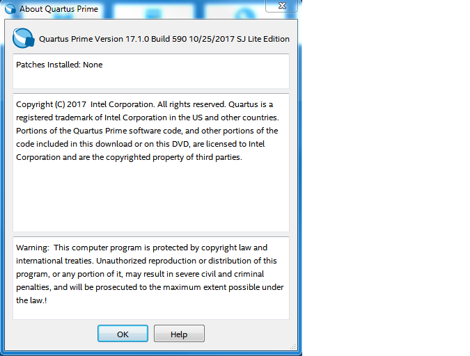
and I'm running Quartus Prime v17.1.0
- Mark as New
- Bookmark
- Subscribe
- Mute
- Subscribe to RSS Feed
- Permalink
- Report Inappropriate Content
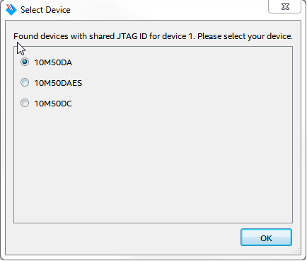
More information. In the User guide, it specifically said "Click “Auto Detect” and select the 10M50DAES."
The actual chip on the Max 10 Development Kit is actually a 10M50DAF484.
So, should I choose 10M50DAES as it stated in the document or choose 10M50DA? Or it doesn't matter??
- Mark as New
- Bookmark
- Subscribe
- Mute
- Subscribe to RSS Feed
- Permalink
- Report Inappropriate Content
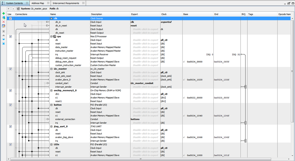
I dig a little bit deeper by going into the Qsys Nios II processor..I don't see any port been exported for UART
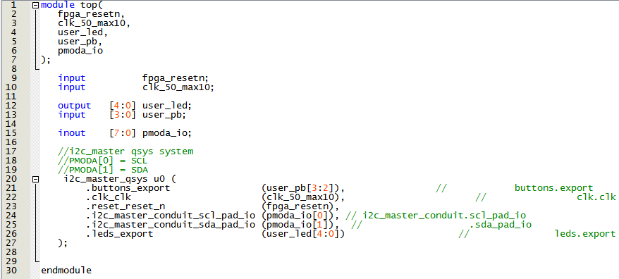
and the top level design doesn't have any UART port either
Could this be the problem? Anyone??
- Mark as New
- Bookmark
- Subscribe
- Mute
- Subscribe to RSS Feed
- Permalink
- Report Inappropriate Content
You don't have to. BTW I see you are connecting the Jtag UART to instruction master (just connect to the Data Master of NIOS II)
- Mark as New
- Bookmark
- Subscribe
- Mute
- Subscribe to RSS Feed
- Permalink
- Report Inappropriate Content
The user guide (attached) for this lab explicitly connected a PC with COM port to the UART port on the Eval board via a USB/UART converter.
In the qsys design, there is no UART at all.
How is this suppose to work then?
- Mark as New
- Bookmark
- Subscribe
- Mute
- Subscribe to RSS Feed
- Permalink
- Report Inappropriate Content
There is a UART in Qsys (Master), in the slave you don't have to have a UART, you need only to download the SOF file to it and will be waiting the commands come from the master boards.
You need to connect the slave board to a PC just to download the .sof file.
- Mark as New
- Bookmark
- Subscribe
- Mute
- Subscribe to RSS Feed
- Permalink
- Report Inappropriate Content
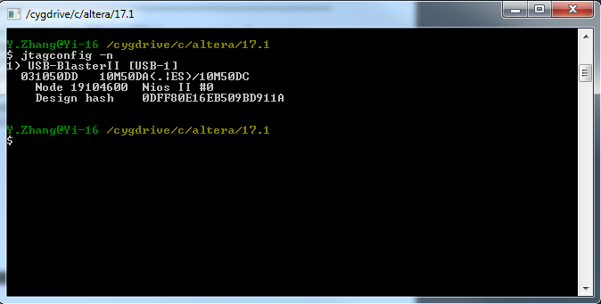
Another thing. I issued jtagconfig –n command in Nios II Command Shell and get the following reply:
It seems to say that I have a Nios II processor with JTAG debug module, but I don't see a node number 0x0C006Exx in the response. This seems to suggest that there's no JTAG UART component?
- Mark as New
- Bookmark
- Subscribe
- Mute
- Subscribe to RSS Feed
- Permalink
- Report Inappropriate Content
You must check SW2 for example it has a pin to choose CFM0, CFM1 or CFM2 image as the first boot image in dual-image configu‐ ration. If the CONFIG_ SEL is set to low, the first boot image is CFM0 image. If CONFIG_SEL is set o high, the first boot image is CFM1 or CFM2 image. This pin is read before user mode and before the nSTATUS pin is asserted
Please check this page:
- Mark as New
- Bookmark
- Subscribe
- Mute
- Subscribe to RSS Feed
- Permalink
- Report Inappropriate Content
@zhangyi17 Hi,
I have the same issue as you. I am stuck at the black Serial port. Did you get this example working?
Thanks in Advance.
- Mark as New
- Bookmark
- Subscribe
- Mute
- Subscribe to RSS Feed
- Permalink
- Report Inappropriate Content
Unfortunately no..If you figure it out, please let me know.
- Mark as New
- Bookmark
- Subscribe
- Mute
- Subscribe to RSS Feed
- Permalink
- Report Inappropriate Content
Hi,
I think the issue is with the nios_firmware.pof. Its programming to QSPI Flash always fails the verify step. I think the firmware is not running at all, DO you have the design files(c files) for nios_firmware.pof
- Subscribe to RSS Feed
- Mark Topic as New
- Mark Topic as Read
- Float this Topic for Current User
- Bookmark
- Subscribe
- Printer Friendly Page

