- Mark as New
- Bookmark
- Subscribe
- Mute
- Subscribe to RSS Feed
- Permalink
- Report Inappropriate Content
Hi,
I am trying to configure DDR3 SDRAM controller with uniphy IP and NIOS II with my custom RTL code. This custom RTL codes generates read/write req with an interface data width of 128 bits.
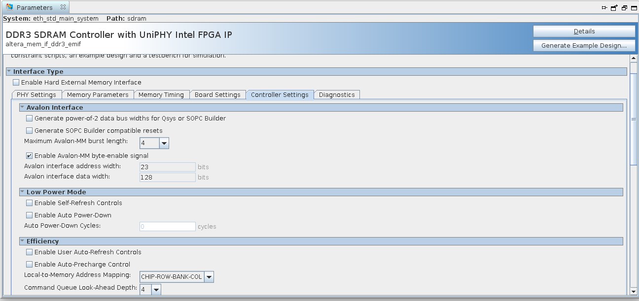
I have attached all the settings I have selected in SDRAM IP, in snapshots(Capture 1,2,3,4).
Problem I am facing: When I generate read req for a burst size of any(say 10), I was exptecting SDRAM to give me data(total of 128 x 10 = 1280 bits) in 10 clock cycles . But I am getting data in different chunks( 128 bits in every 3 or 4 clock cycles), instead of single burst(128 bits in every clock cycles 10 times). This has degraded the performance of my design drastically.
I have also attached the stp result screenshot(result.png) which explains the problem .
Please let me know what is the mistake I might be doing , and how to resolve this so I get 128 bits data every clock cycle.
regards,
Yogesh
Link Copied
- Mark as New
- Bookmark
- Subscribe
- Mute
- Subscribe to RSS Feed
- Permalink
- Report Inappropriate Content
Unless I'm looking at your parameter settings incorrectly, your external memory interface width is set to 32 bits. As such, it would take 4 cycles to get a full 128 bits for a read transfer. The Platform Designer interconnect buffers up the read data to provide the full 128 bits to the host (presumably a Nios processor). The 128 bits is for the internal Avalon interface, not the external memory interface.
- Mark as New
- Bookmark
- Subscribe
- Mute
- Subscribe to RSS Feed
- Permalink
- Report Inappropriate Content
Could you please tell me what should be the correct parameter settings to resolve this issue?
regards,
Yogesh
- Mark as New
- Bookmark
- Subscribe
- Mute
- Subscribe to RSS Feed
- Permalink
- Report Inappropriate Content
@sstrell one more thing I want to add here, Whatever you said makes sense but frequency is also playing role here.
The external memory interface width is 32 bits, but it is DDR running at 300 MHZ.
So at 300MHZ we are getting 64 bits and as AFI clock is 150 MHZ, we should get 128 bits per clock cycle.
Now my design is running at 50 MHZ with a interconnect IP in between, connecting SDRAM and MY IP.
In that case also I should get continuous data and VALID/READY signal.
This is my understanding, please correct me if I am wrong.
- Mark as New
- Bookmark
- Subscribe
- Mute
- Subscribe to RSS Feed
- Permalink
- Report Inappropriate Content
AFI clock is 150Mhz and user design is running 50Mhz, I presume there is avalon MM clock crossing bridge as interconnect between AFI and user clock. Can you check how many burst counts is set in the interconnect ? If that is set only one you should change to 4 or more.
- Mark as New
- Bookmark
- Subscribe
- Mute
- Subscribe to RSS Feed
- Permalink
- Report Inappropriate Content
Yes there is a Interconnect IP, which QSYS puts by default but there is no option to control burst length in that.
But there is a option of "Maximum Burst Length" in SDRAM IP, which is by default set to 4 in SDRAM IP -> controller settings. (Please find attached screenshot of the same)
As per the External Memory Interface Handbook Volume 2:
Page - 328 says that this "Maximum Burst Length" parameter affects the FIFO parameters in Interconnect.
We tried changing it from 4 to 128, still can't see any improvement.
Can you suggest what may be going wrong, which can explain why each transaction in a burst is taking 3 clock cycles, so a burst length of 256 is eventually taking 256*3 = 768 clock cycles.
- Mark as New
- Bookmark
- Subscribe
- Mute
- Subscribe to RSS Feed
- Permalink
- Report Inappropriate Content
Can you replace the interconnect IP to Avalong-MM Clock Crossing Bridge IP from current one ? By default qsys insert interconnect IP without FiFo and burst read/write will be chopped in the interconnect IP.
- Mark as New
- Bookmark
- Subscribe
- Mute
- Subscribe to RSS Feed
- Permalink
- Report Inappropriate Content
I am not able to find the option of replacing the interconnect IP with the Avalon-MM Clock Crossing Bridge IP, can you suggest how to do that?
Instead of this, I tried changing the option Adaptor types in Interconnect requirements from Handshake to FIFO(Please check the attached screenshot).
The problem is now I can't see the trigger on STP which I could in case of Adaptor type is - Handshake.
And if I can't see the STP then it is difficult to see the pattern of Rvalid and Wready signal, so can you please help me in this scenario?
- Mark as New
- Bookmark
- Subscribe
- Mute
- Subscribe to RSS Feed
- Permalink
- Report Inappropriate Content
PFA the screenshot of adaptor settings of default QSYS Interconnect.
- Mark as New
- Bookmark
- Subscribe
- Mute
- Subscribe to RSS Feed
- Permalink
- Report Inappropriate Content
What is STP's trigger you use ? How about just use the Rvalid 's rising edge trigger ?
- Mark as New
- Bookmark
- Subscribe
- Mute
- Subscribe to RSS Feed
- Permalink
- Report Inappropriate Content
@yoichiK_intel My codes are working fine, the only thing now I am trying to do is solving this latency issues coming from this Rvalid/Wready pattern of 2+1 (2 clock cycles low and 1 high) for each burst.
With the default settings, I was able to see the trigger on STP with any conditions as my codes are working.
With this new Interconnect setting change, I was not at all able to see the trigger on STP for any condition.
I tried for RVALID/READ REQUEST signal also but same result.
- Mark as New
- Bookmark
- Subscribe
- Mute
- Subscribe to RSS Feed
- Permalink
- Report Inappropriate Content
- Mark as New
- Bookmark
- Subscribe
- Mute
- Subscribe to RSS Feed
- Permalink
- Report Inappropriate Content
@yoichiK_intel is it allowed to share designs here? as it an IP of the company.
- Mark as New
- Bookmark
- Subscribe
- Mute
- Subscribe to RSS Feed
- Permalink
- Report Inappropriate Content
Did you run the simulation and see same behavior ?
- Mark as New
- Bookmark
- Subscribe
- Mute
- Subscribe to RSS Feed
- Permalink
- Report Inappropriate Content
@yoichiK_intel No I havn't done any simulation with SDRAM IP yet, but on board I am getting correct data.
Can you please guide me how I can run simulation of my IP with SDRAM IP in QSYS as I am new to INTEL tools?
- Subscribe to RSS Feed
- Mark Topic as New
- Mark Topic as Read
- Float this Topic for Current User
- Bookmark
- Subscribe
- Printer Friendly Page