- Mark as New
- Bookmark
- Subscribe
- Mute
- Subscribe to RSS Feed
- Permalink
- Report Inappropriate Content
I have been looking for the assignment names for pins on Arria 10 SoC Development Kit for the last two weeks.
I need to implement a Verilog project using FMCDAQ2 Evaluation board with Arria 10 SoC and I also need to add a UART IP core into the design.
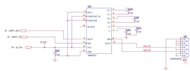
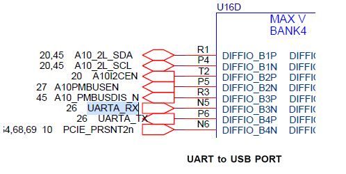
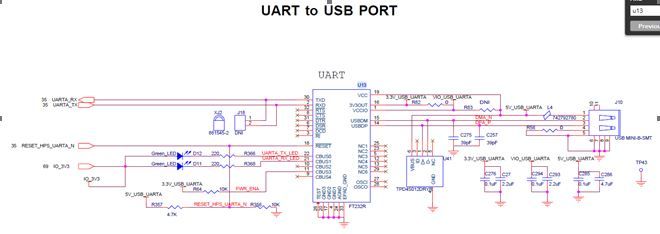
The designs are already done, by which I mean the modules are all designed and ready, but the ADC part of the FMCDAQ2 does not even work somehow, and I can not even find the pin names for UART1 on the board. I can see on the board that the connector is named J10 and the chip is U13, and I have found the schematics, but I can not find the pin names for RX and TX.
Where are the pin assignment names supposed to be?
Link Copied
- Mark as New
- Bookmark
- Subscribe
- Mute
- Subscribe to RSS Feed
- Permalink
- Report Inappropriate Content
Hello,
You can refer to this link for the pinout names in different formats for all the devices:
https://www.intel.com/content/www/us/en/programmable/support/literature/lit-dp.html
Please let me know if you need further assistance.
Thank you,
- Mark as New
- Bookmark
- Subscribe
- Mute
- Subscribe to RSS Feed
- Permalink
- Report Inappropriate Content
I have looked for UARTA on these, but there is none. On the board there is also a DB9 connector which is names J25 on the board itself, so I can use that as well. What I have is a usb-ttl serial converter cable with 4 pins, RX, TX, 5V and GND (here: https://core-electronics.com.au/usb-to-ttl-serial-uart-rs232-adaptor-pl2303hx.html). I just want to connect that to the FPGA and have my design send and receive data through it. Basically I just need 2 pins, a GND pin and a 5V pin. I really find those pinout files very confusing and non-explanatory.
My device is 10AS066, I would appreciate if you could help me.
- Mark as New
- Bookmark
- Subscribe
- Mute
- Subscribe to RSS Feed
- Permalink
- Report Inappropriate Content
Hello,
I am still working on this, once I get a feedback, I will let you know.
Thank you
- Mark as New
- Bookmark
- Subscribe
- Mute
- Subscribe to RSS Feed
- Permalink
- Report Inappropriate Content
- Subscribe to RSS Feed
- Mark Topic as New
- Mark Topic as Read
- Float this Topic for Current User
- Bookmark
- Subscribe
- Printer Friendly Page


