- Mark as New
- Bookmark
- Subscribe
- Mute
- Subscribe to RSS Feed
- Permalink
- Report Inappropriate Content
Hi,
My project need to generate a 16 bit (@1.28Gbp/s data rate) uers data. So I use Serdes to achieve this function. Feed one pair 40M reference to IO/PLL and config SerDes in TX mode.
For the TX_out, I connect them to the Bank 3A/3B, with differential SSTL 1.2V IO standard.
But when I compilate the progarm, pop up an error about DPA. I am so confusing, DPA only includes in RX, I just use FPGA in the TX mode. Where this error come from and how to slove it? Thanks so much, any advice will be appreciated.
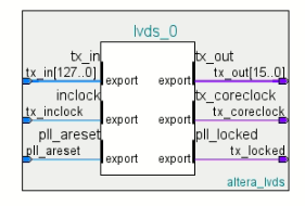
Below is the LVDS SERDES IP's block symbol and the Error in Quartus.
Figure1 error message
Error(19746): The LVDS SERDES IP instance "serdesblockInst|lvds_0|core|arch_inst|channels[0].tx.serdes_dpa_inst" does not have any valid input or output serial port connections.


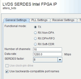
Figure2 LVDS SERDES block symbol Figure3 configuration page
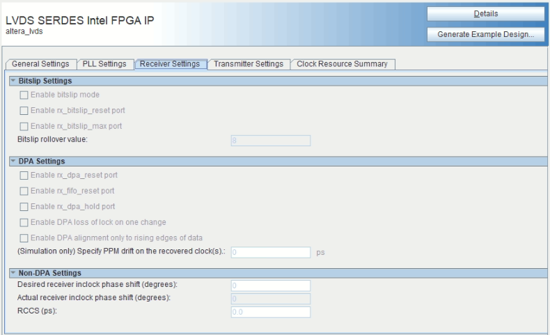
Figure4 configuration page.
Parameter:
1.tx_in[127:0]@ 160Mhz
2.tx_inclock @40Mhz
3.SERDES facor is 8
4.tx_out[15:0] @1.28Gbps
- Mark as New
- Bookmark
- Subscribe
- Mute
- Subscribe to RSS Feed
- Permalink
- Report Inappropriate Content
Hi,
Below could be the reasons for this error:
1) When using dedicated SERDES circuitry, it does not support differential SSTL IO standard. The SERDES requires a direct connection to I/O and hence it can only interface to true LVDS I/O. So, please change IO standard of TX pins to LVDS.
2) Check the reference clock connection. It can be either from the same bank or an adjacent bank.
Regards.
Link Copied
- Mark as New
- Bookmark
- Subscribe
- Mute
- Subscribe to RSS Feed
- Permalink
- Report Inappropriate Content
Hi,
Below could be the reasons for this error:
1) When using dedicated SERDES circuitry, it does not support differential SSTL IO standard. The SERDES requires a direct connection to I/O and hence it can only interface to true LVDS I/O. So, please change IO standard of TX pins to LVDS.
2) Check the reference clock connection. It can be either from the same bank or an adjacent bank.
Regards.
- Mark as New
- Bookmark
- Subscribe
- Mute
- Subscribe to RSS Feed
- Permalink
- Report Inappropriate Content
Hi,
Thanks for your kindly reply. When I change the I/O standard from SSTL to LVDS, the compilation succeeds. And I use pin H1/G1 (bank 3B) as reference clock.
But I still feel vey confused, I double check the IO standard in handbook. It shows SERDES supports SSTL.
Could you please explain more which occasion we can use LVDS and which occasion use differential SSTL-1.2V?
Below is the handbook link.(https://www.intel.com/content/www/us/en/programmable/documentation/vua1487061384661.html#prw1491785518129)
Thanks very much!
Best regards,
Lily
- Mark as New
- Bookmark
- Subscribe
- Mute
- Subscribe to RSS Feed
- Permalink
- Report Inappropriate Content
Hi,
Thanks for your kindly reply. I change the TX I/O standard to LVDS, the compilation passes. And I connect the reference clock to 3B bank (LVDS standard).
But I am still confused. The handbook shows SERDES supports differential SSTL-1.2V. Which kind of occasions can SSTL be used and which occasions can we use LVDS?
Below is the table I copy from SERDES handbook (https://www.intel.com/content/www/us/en/programmable/documentation/vua1487061384661.html#prw1491785518129 ).
Thanks,
Lily
- Subscribe to RSS Feed
- Mark Topic as New
- Mark Topic as Read
- Float this Topic for Current User
- Bookmark
- Subscribe
- Printer Friendly Page


