- Mark as New
- Bookmark
- Subscribe
- Mute
- Subscribe to RSS Feed
- Permalink
- Report Inappropriate Content
I have encountered some problems in the process of learning. I sincerely hope you can spare time to guide me.
- Objective: To obtain 50MHz clock signal by using CycloneV (5CGTFD9E5F35) to output onboard crystal oscillator through phase-locked loop.
- Problems encountered at present: the phase-locked loop was called, pins were allocated and burned into the development board, but the crystal clock signal could not be obtained.
- General process:
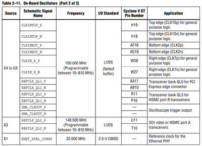
(1) Input pin information found in the manual:
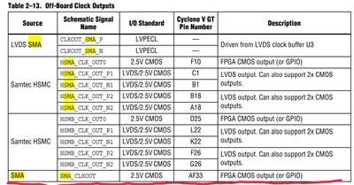
(2) Output pin:
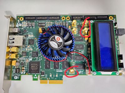
Output position of the corresponding development board:
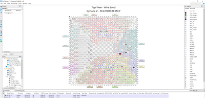
(3) RTL view and pin allocation
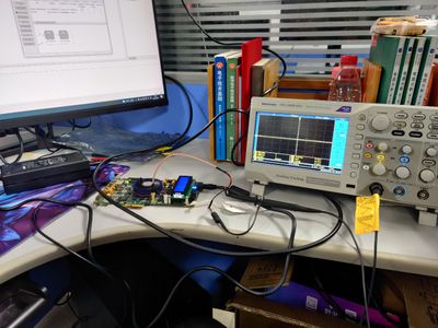
(4) After the program is burned into the development board, the output is connected to the oscilloscope, and the signal can not be obtained.
Link Copied
- Mark as New
- Bookmark
- Subscribe
- Mute
- Subscribe to RSS Feed
- Permalink
- Report Inappropriate Content
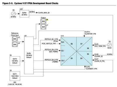
Assuming this is the board you are using (https://www.intel.com/content/www/us/en/products/details/fpga/development-kits/cyclone/v-gt.html), J4 connects to U3, not the FPGA.
- Mark as New
- Bookmark
- Subscribe
- Mute
- Subscribe to RSS Feed
- Permalink
- Report Inappropriate Content
Hello
according to the photo, the OP is connecting J14 (SMA_OUT) to the oscilloscope, it is in fact driven by FPGA pin AF33. Not sure why the configuration doesn't work.
Frank
- Mark as New
- Bookmark
- Subscribe
- Mute
- Subscribe to RSS Feed
- Permalink
- Report Inappropriate Content
Hi,
The input clock of 50MHz should be taken from V28 pin of FPGA and connect to sys_clk of your pll instance. IO standard should be 1.5V CMOS.
Regards
- Subscribe to RSS Feed
- Mark Topic as New
- Mark Topic as Read
- Float this Topic for Current User
- Bookmark
- Subscribe
- Printer Friendly Page

