- Mark as New
- Bookmark
- Subscribe
- Mute
- Subscribe to RSS Feed
- Permalink
- Report Inappropriate Content
Hello,
I want to test the ALTLVDS Megafunction on an Altera NIOS II Development Kit, which includes the CycloneII EP2C35F672C6N FPGA. The intention is to check if I can replace an existing LVDS Transmitter Device on a PCB through an ALTLVDS Megafunction implemented in a Cyclone II FPGA. The FPGA is already on the PCB and after a redesign I could use some of the remaining LEs to implement the LVDS interface to drive a LCD Display. The LVDS Transmitter has 3 channels and a clock channel. The deserialization factor is 7. The test set-up is the following: Intel XScale module with parallel output ports for the Display -> parallel cable to prototyping pins of the NIOS II Development Kit -> LVDS cable from the prototyping pins of the NIOS II Development Kit -> LVDS Display from NEC (640X480, 10,2") The first problem that came up is, that in the Quartus Pin Planner I can´t create more than one or two differential pairs. I´ve got 4 Pins of which i wanted to change the I/O Standard to LVDS. As a result I should get the following output pins: (In my example) tx_out[2] and tx_out[2](n) tx_out[1] and tx_out[1](n) tx_out[0] and tx_out[0](n) tx_outclock and tx_outclock(n) Instead of this I get the following Differential Pairs: tx_out[2] and tx_outclock tx_out[1] and tx_out[0] tx_out[0] and tx_out[1] tx_outclock and tx_out[2] Does anyone have any idea why the pin planner doesn´t creates a positive and a negative pin for each output channel after changing the I/O Standard to LVDS? I´ve already been searching in various Altera Application Notes, Manuals and Handbooks, but I haven´t found anything helpful till now. If anyone has a good tutorial on how to create a LVDS Display Interface in a Cyclone II FPGA it would be helpful too. In the SERDES Transmitter/Receiver (ALTLVDS) Megafunction User Guide I didn´t found the answers to my questions. Thanks for any ideas! Greetings Stefan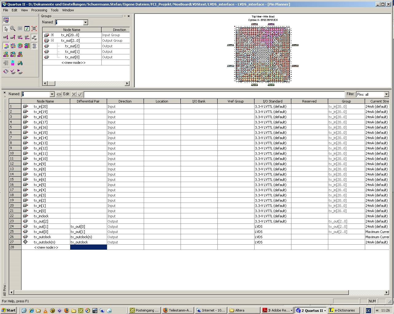
Link Copied
3 Replies
- Mark as New
- Bookmark
- Subscribe
- Mute
- Subscribe to RSS Feed
- Permalink
- Report Inappropriate Content
You don't have to assign the negative pin, it's assigned by the fitter automaticly.
- Mark as New
- Bookmark
- Subscribe
- Mute
- Subscribe to RSS Feed
- Permalink
- Report Inappropriate Content
I talked to an FAE who is a former employee of Altera and he told me, that my problem is a bug in Quartus 8.0 (SP1). To solve the problem I have to delete the db directory of my projekt and change the pin-assignment in the QSF File by myself.
@FvM: Thanks for your efforts!- Mark as New
- Bookmark
- Subscribe
- Mute
- Subscribe to RSS Feed
- Permalink
- Report Inappropriate Content
Yeah, I noticed the same thing in Cyclone III. Quartus II does not create a differential pin but instead uses one of my pre-existing pins.
Strange. Seems like a large bug. Thanks for the tip.
Reply
Topic Options
- Subscribe to RSS Feed
- Mark Topic as New
- Mark Topic as Read
- Float this Topic for Current User
- Bookmark
- Subscribe
- Printer Friendly Page