- Mark as New
- Bookmark
- Subscribe
- Mute
- Subscribe to RSS Feed
- Permalink
- Report Inappropriate Content
Hi
Iam using max10 fpga , having dought regarding to fifo memory block, what is the maximum input clock can be given to fifo ip.
In my project iam using fifo dual clock mode.
write clock = 240 Mhz,
read clock = 60 Mhz,
I studied device data sheet not find any information for the dought.
Thanks in Advance.
Link Copied
- Mark as New
- Bookmark
- Subscribe
- Mute
- Subscribe to RSS Feed
- Permalink
- Report Inappropriate Content
HI Manoj,
The FIFO IP uses the M9K memory component as basic block along with some logic elements. The achievable frequency is determined by overall design in the FPGA.
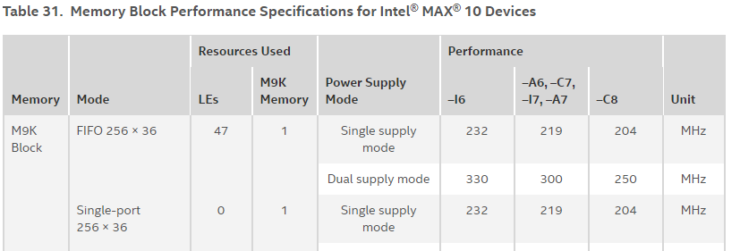
The datasheet provide details of M9K block used in FIFO mode for a fixed configuration. This can be considered as the basis for your estimation.
However, the actual frequency achieved can only be found out from the final Timing Analyzer report.
Regards,
Ashlesha
- Mark as New
- Bookmark
- Subscribe
- Mute
- Subscribe to RSS Feed
- Permalink
- Report Inappropriate Content
Hi Ashlesha,
I found this details in datasheet here they mentioned that we can give input clock upto 300 MHz.
- Mark as New
- Bookmark
- Subscribe
- Mute
- Subscribe to RSS Feed
- Permalink
- Report Inappropriate Content
Hi,
Hope you have got answer to what you are looking for. Is it ok to close this case?
Regards.
- Mark as New
- Bookmark
- Subscribe
- Mute
- Subscribe to RSS Feed
- Permalink
- Report Inappropriate Content
Hi ,
I have changed my design and reduced input clock to 80Mhz, now i am moving with the project. Anyway thanks for the information.
Regards
Manoj
- Subscribe to RSS Feed
- Mark Topic as New
- Mark Topic as Read
- Float this Topic for Current User
- Bookmark
- Subscribe
- Printer Friendly Page
