- Mark as New
- Bookmark
- Subscribe
- Mute
- Subscribe to RSS Feed
- Permalink
- Report Inappropriate Content
Hello.
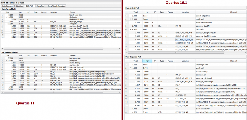
I am trying to describe the time constraints on a project with an 8-bit DDR bus. I took the sample document from the wiki and the accompanying documentation provided by Rysc user (https://fpgawiki.intel.com/wiki/File:Source_Synchronous_Timing_Projects.zip). Example #2 - center alligned receiver, compiled in Qurtus v11 as is - timings are met. I replaced the FPGA on the Cyclone IV _speedgrade 7), increased the frequency of the pll to 150 MHz, corrected the sdc file - timing still ok.
Then I open the same project in new versions of the quartus 13.1,16.1, 18.0 - update the IPs and recompile - the timings are fail!
What can be a reason of it? Few options in my head:
1. In versions higher than 11, fitter was rewritten and he did not optimize the placement so carefully.
2. Added additional checks in timequest, which were simply not performed in earlier versions.
3. Specially worsened the ip-core / fitter, so we must buy more high-speed FPGAs. I can not believe that Cyclone IV can not recieve 150 MHz / 300 Mbs data with altddio_in.
I attach the archive with the edited project for 150 MHz clock.
Link Copied
- Mark as New
- Bookmark
- Subscribe
- Mute
- Subscribe to RSS Feed
- Permalink
- Report Inappropriate Content
Hi,
May I know what device you are using?
In the design, the device is set to AUTO
Thanks
- Mark as New
- Bookmark
- Subscribe
- Mute
- Subscribe to RSS Feed
- Permalink
- Report Inappropriate Content
Yes, i compiled project with "Auto device Selected by Fitter", Select only Cyclone IV E Family, and -7 speedgrade. After your post, i tried manually select and recompile for EP4CE6E22C6, EP4CE115F29I7, 5CEFA9U19I7 with same timing fails (+-300ps).
- Mark as New
- Bookmark
- Subscribe
- Mute
- Subscribe to RSS Feed
- Permalink
- Report Inappropriate Content
I use EP4CE6E22A7 FPGA for compilation. In Q11 timings are met, in Q16.1 - fail.
- Mark as New
- Bookmark
- Subscribe
- Mute
- Subscribe to RSS Feed
- Permalink
- Report Inappropriate Content
Hi,
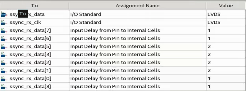
To fix the violation, can you set the following settings in Assignment Editor?
Thanks.
- Mark as New
- Bookmark
- Subscribe
- Mute
- Subscribe to RSS Feed
- Permalink
- Report Inappropriate Content
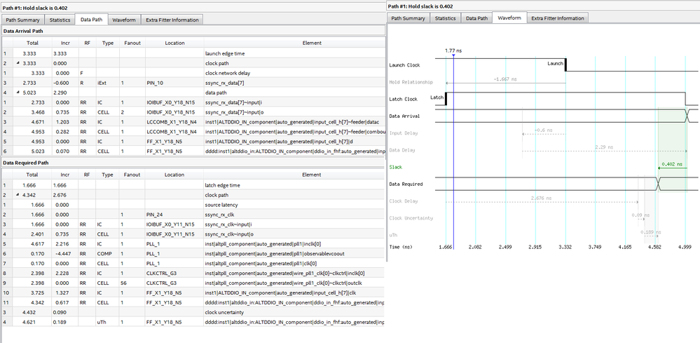
Yes, I can Confirm. With this additional assignment - timing are met with with minimum hold slack 0.402 and setup slack 0.082.
What is the kind of magic? Can you give advice, where and how you know what numbers should be?
Same time, i go another way. I've noticed timequest warning
Warning (176441): The I/O pin RX_DATA[7] cannot meet the timing constraints due to conflicting requirements. The I/O pin is a PLL compensated I/O, but the setup/hold requirements are in conflict with the source PLL mode(source synchronous or ZDB).
Info (176440): Auto delay chain can't change the delay chain setting on I/O pin RX_DATA[6] since it's a PLL compensated pin
Info (176440): Auto delay chain can't change the delay chain setting on I/O pin RX_DATA[5] since it's a PLL compensated pin
Info (176440): Auto delay chain can't change the delay chain setting on I/O pin RX_DATA[4] since it's a PLL compensated pin
Info (176440): Auto delay chain can't change the delay chain setting on I/O pin RX_DATA[3] since it's a PLL compensated pin
Info (176440): Auto delay chain can't change the delay chain setting on I/O pin RX_DATA[2] since it's a PLL compensated pin
Info (176440): Auto delay chain can't change the delay chain setting on I/O pin RX_DATA[1] since it's a PLL compensated pin
Warning (176441): The I/O pin RX_DATA[0] cannot meet the timing constraints due to conflicting requirements. The I/O pin is a PLL compensated I/O, but the setup/hold requirements are in conflict with the source PLL mode(source synchronous or ZDB).
and PLL add huge delay.
Without pll, timings are met..
Then i use LVDS_RX with deser=4 instead of ALTDDIO_IN and just drop 2/4 samples, fitter place input paths in another "faster" location and timing are met too!
Thanks in advance for helping dig deeper in timing constraints and analyse!
- Mark as New
- Bookmark
- Subscribe
- Mute
- Subscribe to RSS Feed
- Permalink
- Report Inappropriate Content
This setting specifies the propagation delay from an input or bidirectional pin to logic and embedded cells within the device. Use this advanced option after you compile a project, check the I/O timing, and determine that the timing is unsatisfactory.
You can use this option to fine-tune the I/O timing of your design and meeting tSU and tH requirements.
- Subscribe to RSS Feed
- Mark Topic as New
- Mark Topic as Read
- Float this Topic for Current User
- Bookmark
- Subscribe
- Printer Friendly Page


