- Mark as New
- Bookmark
- Subscribe
- Mute
- Subscribe to RSS Feed
- Permalink
- Report Inappropriate Content
Hello!
I'm trying to learn about timing analyses and simulation using Quartus Prime lite.
To do so I'm using the following simple design:
module Test01 (input clk, input e0, input e1, output reg q);
reg d1; /* synthesis preserve */
reg d2; /* synthesis preserve */
always @ ( posedge (clk))// source register
d1 <= e0;
always @ ( posedge (clk))// source register
d2 <= d1 & e1;
always @ ( posedge (clk)) // destination register
q <= d2 & 1'b1;
endmodule
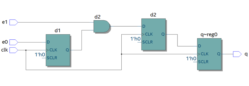
The RTL view of the design looks like this:
In Quartus prime lite 17.1 I then use the Waveform Editor tool:
File->New->University Program VWF.
Inputs e0 and e1 is set to logic 1.
Input clk is set to a clock waveform of period 10ns.
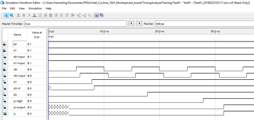
Here are the results of the timing simulation done when choosing
Simulation->Run Timing Simulation
The signals used where selected by choosing:
Edit->insert->Insert Node or bus -> node finder
then, Filter: Post-synthesis, List, then select all signals.
The signals are of 4 categories:
input, output, registered, combinational.
I have a few questions to the simulation result:
Let us start with these two:
1) What is the difference between:
clk of type in and clk~input of type combinational?
2) What is the difference between:
q of type output and q~output of type combinational?
PS! If anyone else likes to run the design or some variation of it and have questions about timing analysis and simulation please feel free to post them in this thread. I guess a lot of beginners will have problems with these two topics.
Link Copied
- Mark as New
- Bookmark
- Subscribe
- Mute
- Subscribe to RSS Feed
- Permalink
- Report Inappropriate Content

Trying again:
RTL netlist view:
Waveform editor:
- Mark as New
- Bookmark
- Subscribe
- Mute
- Subscribe to RSS Feed
- Permalink
- Report Inappropriate Content
Hi Htork,
At first remember to initialize register, seems Quartus has done for you setting them to 0.
Leaving register in an unknown state can be dangerous, when powered up state machine, counters logic can stuck in some unknown unwanted state.
About question:
always @ ( posedge (clk)) // destination register
q <= d2 & 1'b1;
endmodule
is optimized so AND removed from design, if this port added to infer delay design fail.
Question 1:
Clock come from external pin and routed through clock lanes or not. This has some fixed propagation times you can find on data sheet. The two signals are phase shifted by this fixed time.
Question 2:
Q from external pin is delayed of some amount of time related to output buffer from Q of register.
Internal signals are delayed by combinatorial propagation times and register propagation.
First register propagate 1 from input on rising edge.
Second one receive this signal delayed by register propagation time added to combinatorial propagation.
Register output change some time after active clock edge.
Combinatorial logic start propagate when one of input change asyncrounos from clock.
These delay on your image appear as they where few nS wide compared to 10nS clock, on a so simple design on Cyclon10 seems too large.
- Mark as New
- Bookmark
- Subscribe
- Mute
- Subscribe to RSS Feed
- Permalink
- Report Inappropriate Content
I agree that the delay from latch edge of clock to data on register q-pin seems long.
However, since I'm new to this I have nothing to compare with, What should I expect?
What can I do to reduce the delay?
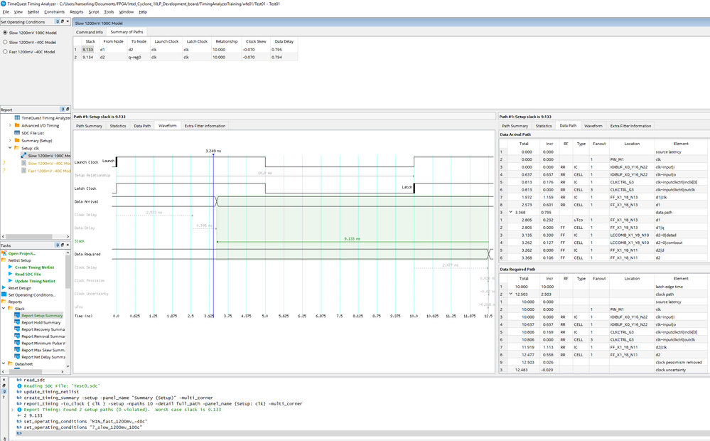
Included image is of the setup slack analysis for the path between register d1 - d2.
It seems that it is the arrival of the latch edge of the clock which is the main reason for the long delay.
The clock is connected to a clock pin on the FPGA.
The other inputs and outputs are connected to nearby pins.
- Mark as New
- Bookmark
- Subscribe
- Mute
- Subscribe to RSS Feed
- Permalink
- Report Inappropriate Content
I can be of little help, I don't know Cyclone10, I don't plan to use. I was happy with MaxII MaxV, Cyclone 2 3 4 5 but MAX 10 this time is driving me crazy.
I am not a beginner but timing closure on this tool seems not so simple and not deterministic.
Try start from there:
https://fpgawiki.intel.com/wiki/Timing_Constraints
https://www.intel.com/content/dam/www/programmable/us/en/pdfs/literature/ug/ug_tq_tutorial.pdf
https://www.intel.com/content/dam/www/programmable/us/en/pdfs/literature/manual/mnl_timequest_cookbook.pdf
For timing closure analysys, I suggest follow competitor course, more aggressive and clear about topics. Intel new class where just slide. (Try a lesson, maybe I am not incline to slide video lesson instead of reading a good manual.)
Best site is this one from a consultant expert, start from bebinner then raise your level up, is clean and is forever one of my references:
https://vhdlwhiz.com/tag/beginner/
- Mark as New
- Bookmark
- Subscribe
- Mute
- Subscribe to RSS Feed
- Permalink
- Report Inappropriate Content
Hi,
Could you please check it again since I am getting different results,
if possible provide the project file(Project->Archive Project)
Regards,
Vicky
- Mark as New
- Bookmark
- Subscribe
- Mute
- Subscribe to RSS Feed
- Permalink
- Report Inappropriate Content
Hi!
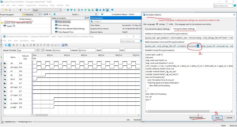
If I'm changing:
quartus_eda --write_settings_files=off --simulation --functional=off.....
to
quartus_eda --write_settings_files=off --simulation --functional=on
I get the same results as you when performing simulation->run timing simulation.
Am I right that this options just turns timing simulation into functional simulation?
That is not what I want to do. I want to see the results after timing is included in the simulation.
Also, I'm using the cyclone 10LP: 10cl025yu256I7G in my design, which is not exactly the same as the one you are using.
I'm sending you the project archieve on email since it seems I can't post it here
- Mark as New
- Bookmark
- Subscribe
- Mute
- Subscribe to RSS Feed
- Permalink
- Report Inappropriate Content
- Subscribe to RSS Feed
- Mark Topic as New
- Mark Topic as Read
- Float this Topic for Current User
- Bookmark
- Subscribe
- Printer Friendly Page


