- Mark as New
- Bookmark
- Subscribe
- Mute
- Subscribe to RSS Feed
- Permalink
- Report Inappropriate Content
Hi.
Iam designing using a Cypress FX3 device (CYUSB3014-BZXC) and a Cyclone IV FPGA(EP4CE115F29C8). The FPGA has a external 50 MHz oscillator. The design shouldrun @ 100 MHz. To do this I have an internal PLL to generate it. TheFX3 device has a 32 bits source synchronous interface running @100MHz clockcoming from the FPGA. The FX3 device receive the data center-aligned. As guidance for theport name I has the following ones:
moduleSLAVE_FIFO_STREAM_IN(
   input              CLOCK_50,      //input clp 50 Mhz
   inout            FX3_DQ,         //data bus
   output               FX3_faddr,       //output fifo address
   output             FX3_slrd,        //output read select
   output             FX3_slwr,        //output write select
   input              FX3_flaga,      //full flag
   input              FX3_flagb,      //partial full flag
       input              FX3_flagc,      //empty flag
   input              FX3_flagd,     //empty partial flag
   output             FX3_sloe,      //output output enable select
   output             FX3_CLK,      //output clk 100 Mhz and 180 phase shift
   output             FX3_slcs,      //output chip select
   output             FX3_pktend, //output pkt end
   output               FX3_PMODE,
   output             FX3_RESET,
   output             FX3_PMODE_2 //used fordebugging
);
I already set thenext into my design: 1) Analtddio_out_component to shift the out clock 180° (Connected the datain_h(1'b0)and datain_l(1'b1) to make it) 2) I already set theoutput parallel interface as: "set_instance_assignment -nameFAST_OUTPUT_REGISTER ON" 3) My SDCconstraints are the next ones:
set_time_format-unit ns -decimal_places 3
#**************************************************************
# Create Clock
#**************************************************************
create_clock -nameCLOCK_50M -period 20.000
create_generated_clock\
 -nameCLOCK_100M \
 -multiply_by 2\
 -source}] \
  }]
#**************************************************************
# Create GeneratedClock
#**************************************************************
# Put a generatedclock on output clock port to be referenced by set_output_delay constraints. Note the -invert option, which says the clock is being inverted on theway out.  This is important
# since Quartusdoesn't recognize the DDR output with VCC/GND switched as inverting the clock
create_generated_clock-source }] -nameCLOCK_FX3  -invert
set_false_path -to
#Constrain the PLLautomatically
derive_pll_clocks-create_base_clocks
#**************************************************************
# Set ClockUncertainty
#**************************************************************
derive_clock_uncertainty
################################################################################
#Parameters
################################################################################
# Specify themaximum external clock delay to the FPGA
set FX3_CLKs_max 0
# Specify theminimum external clock delay to the FPGA
set FX3_CLKs_min 0
# Specify themaximum external clock delay to the external device
set FX3_CLKd_max 0
# Specify theminimum external clock delay to the external device
set FX3_CLKd_min 0
# Specify themaximum setup time of the external device
set FX3_tSU 2
# Specify theminimum setup time of the external device
set FX3_tH 0.5
# Specify themaximum board delay
set FX3_BD_max 0
# Specify theminimum board delay
set FX3_BD_min 0
# Specify themaximum clock-to-out of the external device
set FX3_tCO_max 9
# Specify theminimum clock-to-out of the external device
set FX3_tCO_min 2
################################################################################
#Output constraints
################################################################################
set_output_delay-clock CLOCK_FX3 -max
set_output_delay-clock CLOCK_FX3 -min   -add_delay
################################################################################
#Input constraints
################################################################################
set_input_delay-clock CLOCK_FX3 -max
set_input_delay-clock CLOCK_FX3 -min
I have beenreviewing the Timequest guides provided in the AlteraWiki and the correspondingmanuals. But I cannot evacuate the next doubt: As the design has aclock offset of 180° between the launch and the latch clock, (relative to theoutputs to the device) I do not know which is the right way to constraint this.I should use a set_multicycle_path command? The design has a synchonizer betweenthe register coming from the external device, but I do not know how tell thisto Timequest. I attached a zippedfile for the design if this is easier to understand. Thanks in advance. Franco
Link Copied
- Mark as New
- Bookmark
- Subscribe
- Mute
- Subscribe to RSS Feed
- Permalink
- Report Inappropriate Content
One note: you create PLL generated clocks and also call derive_pll_clocks. You should only do one or the other.
Other than that, this looks OK. The output generated clock is the latch clock and the -invert provides the 180 degree phase shift. You don't need multicycle here (that's only needed on an output in the edge aligned case). So what is the issue or problem you are having?- Mark as New
- Bookmark
- Subscribe
- Mute
- Subscribe to RSS Feed
- Permalink
- Report Inappropriate Content
Hi Strell,
Thank you for you review. The issue that I have, is related to the clock relationship. As the internal register are clocked by the internal 100MHz and the external device is a clocked by a 180° 100 MHz offset, the design has a setup relationship of 5 ns instead or original 10 ns for the output and input register connected to the output/input pin. I attached a figure for this violation. https://alteraforum.com/forum/attachment.php?attachmentid=15430&stc=1 For instante, the FX3_flaga, FX3_flaga, FX3_flaga, FX3_flaga are signals cominf from the external device.always @(posedge clk_100, negedge reset_)begin
if(!reset_)begin
flaga_d <= 1'd0;
flagb_d <= 1'd0;
flagc_d <= 1'd0;
flagd_d <= 1'd0;
end else begin
flaga_d <= FX3_flaga;
flagb_d <= FX3_flagb;
flagc_d <= FX3_flagc;
flagd_d <= FX3_flagd;
end
end The register connected to the FX3_flagx to flaga_x has a setup relationship of 5 ns. Which is the right way to constraint this? a set_multicycle_path between them? or a set_false_path directive?
- Mark as New
- Bookmark
- Subscribe
- Mute
- Subscribe to RSS Feed
- Permalink
- Report Inappropriate Content
But this is what you want, right? Or are you saying that the downstream device should have a cycle and a half for capture?
If it should be 5 ns, you can't use multicycle because that is just loosening the timing requirements (extending it to a cycle and a half = 15 ns). If it needs to be 5 ns, you need to find other ways to make it work, such as launching the data earlier or latching the data later using phase shifts in the PLL. If you can do that, then you may need to use multicycle to compensate for it so that the timing analyzer chooses the correct edges for its analysis. Have you looked at this training at all: https://www.altera.com/support/training/course/ocss1000.html- Mark as New
- Bookmark
- Subscribe
- Mute
- Subscribe to RSS Feed
- Permalink
- Report Inappropriate Content
I already taken the webinar proposed. It is very interesting. I am using the DDIO OUTPUT register to drive the shifted clock :
altddio_out_component	altddio_out_component_inst (
	.datain_h(1'b0),
	.datain_l(1'b1),
	.outclock(clk_100),
	.dataout(FX3_CLK)
	);
I am following an example provided by Cypress doing this, but the parallel interface is not driven by another altddio component, instead is driven as a common tristate signal: assign FX3_DQ = (slwr_streamIN_d1_) ? 32'dz : data_gen_stream_in; I note now that the ddio register approach for SDR is the next one: https://www.alteraforum.com/forum/attachment.php?attachmentid=15438 Maybe it is needed to use another altddio_out component to drive the FX3_DQ inout bus?
- Mark as New
- Bookmark
- Subscribe
- Mute
- Subscribe to RSS Feed
- Permalink
- Report Inappropriate Content
You didn't answer my question. What is the timing requirement you need at the downstream device? Should it be 5 ns because of the 180 degree phase shift or does it need to be 15 ns (a cycle and a half)?
- Mark as New
- Bookmark
- Subscribe
- Mute
- Subscribe to RSS Feed
- Permalink
- Report Inappropriate Content
I attached a timing diagram for this interface:
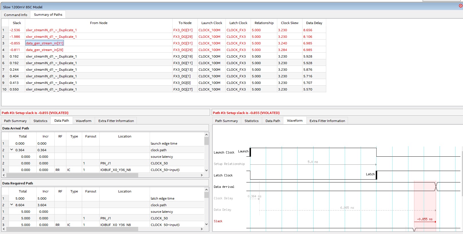
https://www.alteraforum.com/forum/attachment.php?attachmentid=15440 The clock is drived by the FPGA. The external device latchs the data in the clock rising edge. For this reason it is needed to make a 180° phase offset. I guess that this implies a 5 ns for the setup relationship. How it is possible to implement this interface due the delay timing? Below is the picture for the paths failing, which are the output register connected to the data interface https://www.alteraforum.com/forum/attachment.php?attachmentid=15441- Mark as New
- Bookmark
- Subscribe
- Mute
- Subscribe to RSS Feed
- Permalink
- Report Inappropriate Content
OK, well if this is the case, then the problem is specific to those 4 paths failing timing. You do not want to add multicycle. All the other output data paths look fine. The sources for those 4 paths are different from the rest. Why? The path you highlight has a very large data delay internal to the device (over 2 ns). Are you forcing the source logic to a particular part of the device and then the data delay is incurred by having to get over to pin T7?
At this point, you need to use traditional timing closure techniques to fix these paths. The output interface itself does not seem to be the problem.- Mark as New
- Bookmark
- Subscribe
- Mute
- Subscribe to RSS Feed
- Permalink
- Report Inappropriate Content
Ok, understand. Actually no. It is a 32 bits bus. Some lines (corresponding to lanes 31 & 29) are failing. But the entirely bus is assigned in th same way.
I am reviewing the report deeply. I can see some differences in the datapath regarding to the other lanes, but I think any was forced by me. I attached the report file which I was researching. As you mentioned exist more than 2 nS of difference but it was not my intention to do it.- Mark as New
- Bookmark
- Subscribe
- Mute
- Subscribe to RSS Feed
- Permalink
- Report Inappropriate Content
I can see that just the failing lines are the lines conected to pins T7 and T8. Those are VREF pins. All the other are not. It this can be the issue? I heard about the higher capacitance for these pins. Maybe is this the problem? Can this be mitigated in some way?
- Subscribe to RSS Feed
- Mark Topic as New
- Mark Topic as Read
- Float this Topic for Current User
- Bookmark
- Subscribe
- Printer Friendly Page