- Mark as New
- Bookmark
- Subscribe
- Mute
- Subscribe to RSS Feed
- Permalink
- Report Inappropriate Content
Hi all.
I have some things to discuss about Source Synchronous representation in TimeQuest.
I attached the project, which is slightly modified version of Source Synchronous Analysis with TimeQuest by Ryan Scoville - https://forums.intel.com/s/createarticlepage?articleid=a3g0P0000005RIKQA2&artTopicId=0TO0P000000MWKBWA4&action=view
The project is an example of Source Synchronous design,
where FPGA is a transmitter, it shifts the clock, it is the same edge transfer mode, DDR. Inside the project there is a PLL which shifts the clock by 90 degrees, DDIO and registers for creation data to transmit. Clock goes out also using DDIO.
Constraints are as in the example, only set_false_path was added to leave FR and RF paths (for setup) away from analysis.
So, what is the discussion.
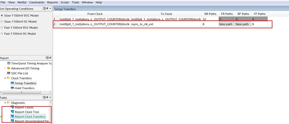
First of all, in order to check timing, I used Report Clock Transfers command
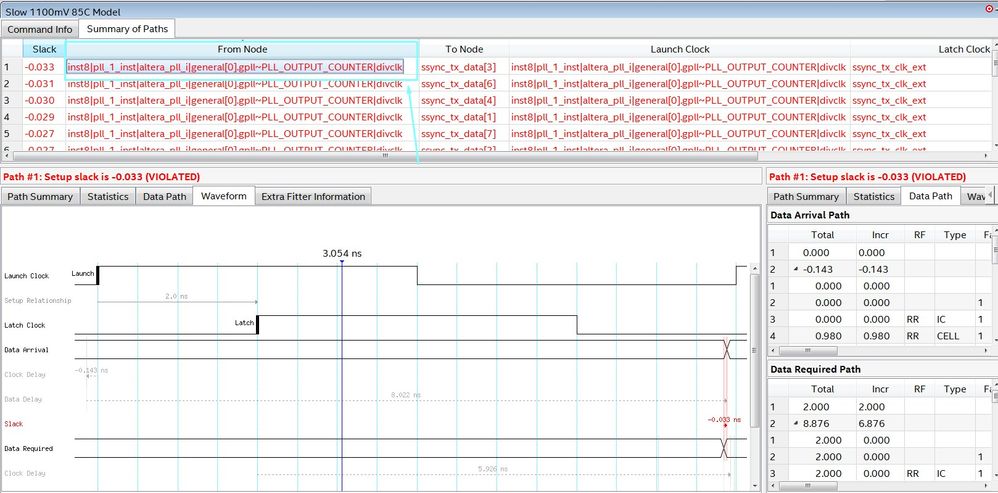
and report_timing command on the clock transfer between system clock (inst8|pll_1_inst|altera_pll_i|general[0].gpll~PLL_OUTPUT_COUNTER|divclk) and clock going out of FPGA (ssync_tx_clk)
The first interesting thing is - it could be seen that Quartus successfully
detects paths where Launch clock is FPGA system clock which creates data and Latch clock is shifted version of system clock which goes out from FPGA port and which we described using create_generated_clock command. But it could be seen that Quartus chose PLL output - (inst8|pll_1_inst|altera_pll_i|general[0].gpll~PLL_OUTPUT_COUNTER|divclk) as a starting point (from Node column).
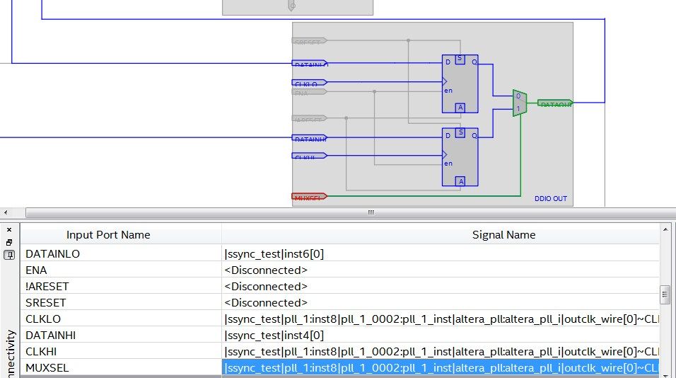
Here is a figure from Technology Map viewer to represent one of those paths
And the first question is - why it is so? Why PLL output is the starting point of that path?
My explanation is that it is because of mux located inside DDIO block in Cyclone V. The output of that mux is controlled by clock from PLL, and this mux naturally enables DDR regs to go out to IO Buf. But I'm asking if it is a right explanation.
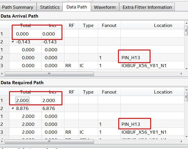
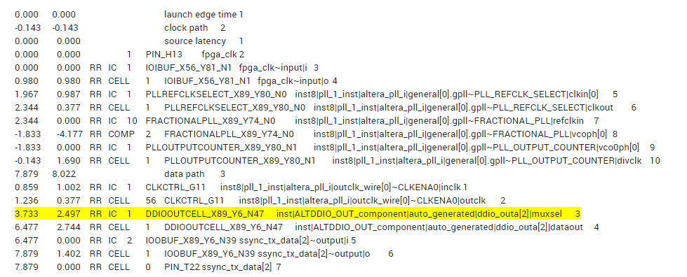
The second thing is that if we inspect that path - look at the detailed Data Path report
we will see in my opinion a bit strange behaviour - in Data Required Path
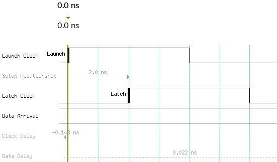
Clock starts from input pin, but starts at 2 ns. It is not what should be in a real world, because timing starts in Data Arrival Path at 0 ns time -
and clock gets shifted inside PLL, and the right report for Data Required Path should start from 0 ns time and should get a 2 ns inside the PLL.
So the second question is - why it is so? There is no reflection of clock phase shift inside detailed path analysis - the shift is incorporated at the start of the analysis.
Thanks in advance.
--
Best regards,
Ivan
Link Copied
- Mark as New
- Bookmark
- Subscribe
- Mute
- Subscribe to RSS Feed
- Permalink
- Report Inappropriate Content
Can you post just the .sdc file?
You need a false path on your output clock path because the tool is looking at this path still as a data path:
set_false_path -to [get_ports ssync_tx_clk_ext]
The false paths you mention you created should be from the data clock (the clock that is driving out data) to ssync_tx_clk_ext, something like this:
set_false_path -setup -rise_from [get_clocks data_clk] -fall_to [get_clocks ssync_tx_clk_ext]
set_false_path -setup -fall_from [get_clocks data_clk] -rise_to [get_clocks ssync_tx_clk_ext]
set_false_path -hold -rise_from [get_clocks data_clk] -rise_to [get_clocks ssync_tx_clk_ext]
set_false_path -hold -fall_from [get_clocks data_clk] -fall_to [get_clocks ssync_tx_clk_ext]
Can you confirm this is how you did your constraints?
#iwork4intel
- Mark as New
- Bookmark
- Subscribe
- Mute
- Subscribe to RSS Feed
- Permalink
- Report Inappropriate Content
Hi sstrell.
Yes, my .sdc file looks like that:
create_clock -period 8.0 -name fpga_clk [get_ports fpga_clk]
# Constrains PLL outputs. One output has 90 degree phase-shift for transmit clock
derive_pll_clocks
derive_clock_uncertainty
# Put a generated clock on output clock port to be referenced by set_output_delay constraints
create_generated_clock -source [get_pins {inst8|pll_1_inst|altera_pll_i|general[1].gpll~PLL_OUTPUT_COUNTER|divclk}] -name ssync_tx_clk_ext [get_ports {ssync_tx_clk}]
set_output_delay -clock ssync_tx_clk_ext -max 0.9 [get_ports {ssync_tx_data[*]}]
set_output_delay -clock ssync_tx_clk_ext -min -1.0 [get_ports {ssync_tx_data[*]}]
set_output_delay -clock ssync_tx_clk_ext -max 0.9 [get_ports {ssync_tx_data[*]}] -clock_fall -add_delay
set_output_delay -clock ssync_tx_clk_ext -min -1.0 [get_ports {ssync_tx_data[*]}] -clock_fall -add_delay
set_false_path -fall_from [get_clocks {inst8|pll_1_inst|altera_pll_i|general[0].gpll~PLL_OUTPUT_COUNTER|divclk}] -rise_to [get_clocks ssync_tx_clk_ext] -setup
set_false_path -rise_from [get_clocks {inst8|pll_1_inst|altera_pll_i|general[0].gpll~PLL_OUTPUT_COUNTER|divclk}] -fall_to [get_clocks ssync_tx_clk_ext] -setup
set_false_path -fall_from [get_clocks {inst8|pll_1_inst|altera_pll_i|general[0].gpll~PLL_OUTPUT_COUNTER|divclk}] -fall_to [get_clocks ssync_tx_clk_ext] -hold
set_false_path -rise_from [get_clocks {inst8|pll_1_inst|altera_pll_i|general[0].gpll~PLL_OUTPUT_COUNTER|divclk}] -rise_to [get_clocks ssync_tx_clk_ext] -hold
set_false_path -to [get_ports {ssync_tx_clk}]
So I can confirm that my constraints are like you suggested.
--
Best regards,
Ivan
- Mark as New
- Bookmark
- Subscribe
- Mute
- Subscribe to RSS Feed
- Permalink
- Report Inappropriate Content
This is a stupid question, but are the correct clocks from the PLL connected to the data DDIO (and clock DDIO) in your design? Like you said, it doesn't make sense that you're seeing data path analysis with a PLL output as the from node.
#iwork4intel
- Mark as New
- Bookmark
- Subscribe
- Mute
- Subscribe to RSS Feed
- Permalink
- Report Inappropriate Content
Hi sstrell.
Yes, I'm sure, that clocks from the PLL are connected properly to the DDIO. I attached a simple project, and just've checked it.
Thank you.
--
Best regards,
Ivan
- Mark as New
- Bookmark
- Subscribe
- Mute
- Subscribe to RSS Feed
- Permalink
- Report Inappropriate Content
Hi sstrell.
Is there any update for an issue, did you see the attached project?
--
Best regards,
Ivan
- Mark as New
- Bookmark
- Subscribe
- Mute
- Subscribe to RSS Feed
- Permalink
- Report Inappropriate Content
Hi Ivan,
The DATAINHI and DATAINLO have constant value and the output of the PLL is connected to the MUXSEL/CLKHI/CLKLO of the ddio. Besides this, the clock relationship is 2ns, which is why you see 2ns in the latch edge time under Data Required Path.
Thanks.
- Mark as New
- Bookmark
- Subscribe
- Mute
- Subscribe to RSS Feed
- Permalink
- Report Inappropriate Content
Hi YY.
Thank you.
As about your answer.
About my first question - as for the data path, there are no constant values on DATAINHI and DATAINLO. DATAINHI and DATAINLO connected to synchronizers, which are in turn connected to input ports.
And yes, output of the PLL is connected to the MUXSEL, CLKHI and CLKLO.
So it is a strange situation, where as I understand, we need to consider the whole DDIO and a mux as its ending element as a one trigger-like sequential element, which launches data to the output port.
My question was is it a right explanation, or not. It looks like previous customer (sstrell) who tried to answer that question said "it doesn't make sense that you're seeing data path analysis with a PLL output as the from node."
So it is an interesting case, isnt' it?
As my second question - maybe my question was not descriptive enough, my question was not why I'm seeing 2ns in the latch edge time under Data Required Path,
but why in the Detailed Data Path report we start the clock Path from the input pin and it starts from 2 ns?
Again, I can post my question:
"clock gets shifted inside PLL, and the right report for Data Required Path should start from 0 ns time and should get a 2 ns inside the PLL.
So the second question is - why it is so? There is no reflection of clock phase shift inside detailed path analysis - the shift is incorporated at the start of the analysis."
I can try to explain that - for example - "clock shifts inside PLL aren't represent in the timing path report".
--
Best regards,
Ivan
- Mark as New
- Bookmark
- Subscribe
- Mute
- Subscribe to RSS Feed
- Permalink
- Report Inappropriate Content
Hi,
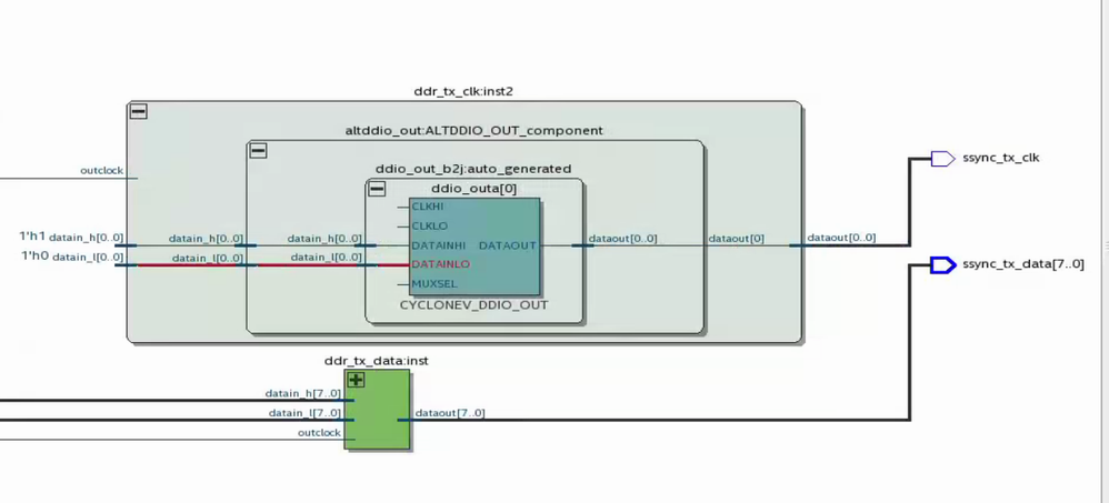
From the design, the DATAINHI and DATAINLO are connected to 1'h1 and 1'h0.
In general, you would see clock sources as the starting point of timing paths in a "clock-as-data" scenario, when a clock feeds a data input pin of a register (or an output pin with a "data-like" constraint like set_output_delay).
Looking at the circuit in netlist viewer, it seems that the PLL output is driving "CLKHI", "CLKLO" and "MUXSEL" inputs of the DDIO_OUT blocks. Looking at the timing path report (pasted below), it looks like the MUXSEL input is modeled as a data input (as opposed to a clock input). So, we have a "clock-as-data" path, where the PLL output clock is driving the ssync_tx_data pin (via MUXSEL of the DDIO), which has a set_output_delay constraint, creating a valid timing path.
So, Timing Analyzer behavior looks correct.
The clock is 0ns from input pins, get shifted by 2ns through the PLL . This clock inst8|pll_1_inst|altera_pll_i|general[1].gpll~PLL_OUTPUT_COUNTER|divclk has 2ns delay compared to inst8|pll_1_inst|altera_pll_i|general[0].gpll~PLL_OUTPUT_COUNTER|divclk, which is why the latch clock edge is 2ns but not 0ns.
Thanks.
- Mark as New
- Bookmark
- Subscribe
- Mute
- Subscribe to RSS Feed
- Permalink
- Report Inappropriate Content
Hi YY.
Thank you very much for your answer.
I suppose I need to summarise the case. I think that our discussion could be at that point helpful for the community.
First of all, I again can repeat - "as for the data path, there are no constant values on DATAINHI and DATAINLO". But yes, DATAINHI and DATAINLO are indeed connected to 1'h1 and 1'h0, but it's NOT a data path,
it's a clock path, and it's excluded from the timing with set_false_path constraint, as I mentioned earlier. So there is no need to think about it and this has nothing to do with the case.
As about your further explanation, thank you very much, it's like I explained it in my post here, so you confirmed my guess with a detailed explanation!
But final problem - I'm still observe I can't describe my problem properly because what you wrote is obvious-
again, my question is - Why in the detailed timing report the phase shift of clock (2 ns) is introduced at the beginning (from the input port), not after it enters PLL and gets shifted inside of it.
I understand and yes, you are right, latch edge of course is 2 ns, it's because of the shift, but in DETAILED timing report we observe path from the input pin, and the shift should be in that case INSIDE the PLL,
not on the pin.
Thank you very much again.
--
Best regards,
Ivan
- Subscribe to RSS Feed
- Mark Topic as New
- Mark Topic as Read
- Float this Topic for Current User
- Bookmark
- Subscribe
- Printer Friendly Page
