- Mark as New
- Bookmark
- Subscribe
- Mute
- Subscribe to RSS Feed
- Permalink
- Report Inappropriate Content
I have instantiated a sigle multiplier as below:
`timescale 1 ns / 1 ps

module modules(clk,
			  rst,
			  i_conv_clken,
           i_input_data_a,
           i_input_data_b,
           o_mult_result );


input clk,rst,i_conv_clken;
input signed [7:0] i_input_data_a,i_input_data_b;

output reg signed[20:0] o_mult_result;
wire [15:0] out;

lp_mult lp_mult_component (
   .clock(clk),
   .clken(i_conv_clken),
   .dataa (i_input_data_a),
   .datab (i_input_data_b),
   .result (out)
   );


always@(posedge clk or negedge rst)
begin
 if(!rst)
  begin
    o_mult_result<=0;
  end
 else
  begin
   o_mult_result<= out;
  end
end
endmodule
constraints - 500 Mhz
read_sdc -hdl
create_clock -name clk -period 2 [get_ports {clk}]
Results I got is:
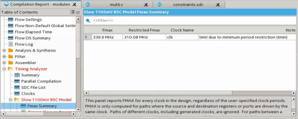
Fmax=906Mhz
Restricted Fmax=605Mhz
but in below document its mentioned that an independent 9x9 multiplier can achieve 300 Mhz max in cyclone V GT.
page 44 in below document:
https://www.intel.com/content/dam/www/programmable/us/en/pdfs/literature/hb/cyclone-v/cv_51002.pdf
So, am I doing something wrong in knowing the max frequency that can be achieved in cyclone V GT?
If yes how to find out the max frequency of a DSP in cyclone v GT?
Link Copied
- Mark as New
- Bookmark
- Subscribe
- Mute
- Subscribe to RSS Feed
- Permalink
- Report Inappropriate Content
Hi,
The verilog above instantiate lp_mult; the source file for the lp_mult is required in order to compile the design. Could you provide the design QAR for investigation? To create the QAR file, click on Project > Archive Preoject > Archive.
Thanks.
Best regards,
KhaiY
- Mark as New
- Bookmark
- Subscribe
- Mute
- Subscribe to RSS Feed
- Permalink
- Report Inappropriate Content
Hi,
Please find the qar file as requested.
Thankyou
- Mark as New
- Bookmark
- Subscribe
- Mute
- Subscribe to RSS Feed
- Permalink
- Report Inappropriate Content
Hi,
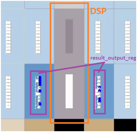
If you locate the node in the Chip Planner, you will see that the register is outside of the DSP. Thus, this is not limited by the performance of the DSP.
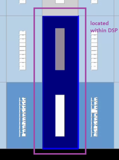
Changing the DSP pipeline to 3, you will see that the result_extra0_reg[15:0] that is located in the DSP requires 3.225 for the min period
Thanks.
Best regards,
KhaiY
- Mark as New
- Bookmark
- Subscribe
- Mute
- Subscribe to RSS Feed
- Permalink
- Report Inappropriate Content
Hi,
I have modified my code and is facing new issue with resect to DSP resource utilization.
I am sharing archieve of my sample code.
Here I have instantiated 48 lpm_mult IP. Each lpm_mult takes two 8 bit inputs , and will provide 16 bit output.
Ideally tool should use 16 DSPs since each DSP in cyclone V has three 9x9 multipliers.
But it is using 24 DSPs(with each DSP using sum of two 18x18 multipliers)
If this is the case ,I will face shortage of DSPs in my top level.
So, I want the tool to use three 9x9 for each DSP(since i am only doing 8x8 multiplication).
1)I thought tool might be using more since its available, but it is not the case.Say If i instantiate 685 9x9 multipliers , It will use 342 DSPs(100 % usage- each DSP using sum of two 18x18), and for one more 9x9(i.e 685 th multiplier) it will use ALMs.
As a result there is drop in my required frequency . Tool should have used 3 9x9 atleast in this case since there are no more DSPs, to achieve required design right?
2) Am I doing something wrong in the instantiation , so that tool is not understanding that it should use 1 DSP for 3 instances of 9x9 lpm_mults? If yes, please tell me how to make tool use it so?
3) I want to know how to use DSPs in different operational modes mentionaed in below document (page number 3-10)
https://www.intel.com/content/dam/www/programmable/us/en/pdfs/literature/hb/cyclone-v/cv_5v2.pdf
Please help me with this issue.
Thankyou,
regards.
Yogesh
- Mark as New
- Bookmark
- Subscribe
- Mute
- Subscribe to RSS Feed
- Permalink
- Report Inappropriate Content
Hi Yogesh,
The initial question is about the timing Fmax of the design with DSP; it has been answered. Can you create a new forum post for new question? This is to make sure that each forum post has only one question so that other customers with the similar question/issue/problem can find the solution/explanation easily.
Thanks.
Best regards,
KhaiY
- Mark as New
- Bookmark
- Subscribe
- Mute
- Subscribe to RSS Feed
- Permalink
- Report Inappropriate Content
Hi Yogesh,
May I know if you have any concerns?
Thanks.
Best regards,
KhaiY
- Mark as New
- Bookmark
- Subscribe
- Mute
- Subscribe to RSS Feed
- Permalink
- Report Inappropriate Content
Hi,
I have created a new post for that particular question, and I am working on that.
Thankyou,
regards,
Yogesh
- Mark as New
- Bookmark
- Subscribe
- Mute
- Subscribe to RSS Feed
- Permalink
- Report Inappropriate Content
Hi Yogesh,
Sure. Thanks for the update.
Best regards,
KhaiY
- Mark as New
- Bookmark
- Subscribe
- Mute
- Subscribe to RSS Feed
- Permalink
- Report Inappropriate Content
Hi Yogesh,
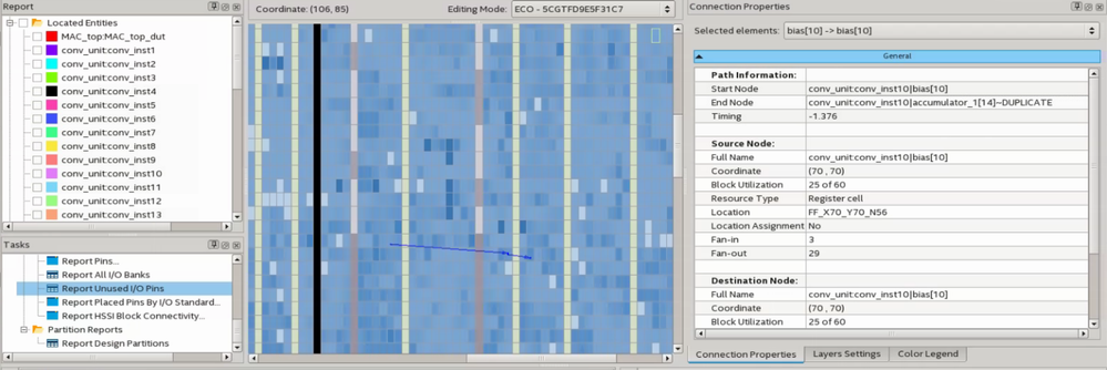
If you locate the path that failed timing in the Chip Planner, you will notice that the path is in the core logic area but not inside the IP. As explained earlier, this is not limited by the DSP performance, you have to look into each of the path and see why it fails to meet the desired frequency.
Take an example of From node: conv_unit:conv_inst10|bias[10], To node: conv_unit:conv_inst10|accumulator_1[14]~DUPLICATE, you can see that both node are not located inside the DSP (Grey color block)
I notice that you constrained the clock only without constraining the I/O port. Even if you get the STA clean result after fixing the violation, the design might not operate as intended as you didnt consrain how the FPGA interact with external device. In this case, you have to make sure that the all the necessary constraints are added in the SDC, then you can start to fix the timing violation in the failing path.
You may refer to Intel Quartus Prime Timing Analyzer Cookbook : https://www.intel.com/content/dam/www/programmable/us/en/pdfs/literature/manual/mnl_timequest_cookbook.pdf. This document explains how to constrain clock, I/O port, and some timing exceptions that you might want to apply in the design.
Thanks.
Best regards,
KhaiY
- Mark as New
- Bookmark
- Subscribe
- Mute
- Subscribe to RSS Feed
- Permalink
- Report Inappropriate Content
Hi,
Do you have any updates?
Thanks.
Best regards,
KhaiY
- Mark as New
- Bookmark
- Subscribe
- Mute
- Subscribe to RSS Feed
- Permalink
- Report Inappropriate Content
Hi,
We do not receive any response from you to the previous question/reply/answer that I have provided. Please post a response in the next 15 days to allow me to continue to support you. After 15 days, this thread will be transitioned to community support. The community users will be able to help you with your follow-up questions.
Thanks.
Best regards,
KhaiY
- Subscribe to RSS Feed
- Mark Topic as New
- Mark Topic as Read
- Float this Topic for Current User
- Bookmark
- Subscribe
- Printer Friendly Page


