- Mark as New
- Bookmark
- Subscribe
- Mute
- Subscribe to RSS Feed
- Permalink
- Report Inappropriate Content
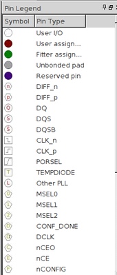
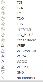
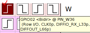
Could someone please tell me what is the function of and how to use following pins of the FPGA, as follows picture?
If there exists a document to explain it, could you please share the document?
Thank you very much.
Link Copied
- Mark as New
- Bookmark
- Subscribe
- Mute
- Subscribe to RSS Feed
- Permalink
- Report Inappropriate Content
Every device family has a device handbook that goes into detail on the functions of the I/O. Just search the documentation for your selected device.
Is there something here in particular you want to know about?
- Mark as New
- Bookmark
- Subscribe
- Mute
- Subscribe to RSS Feed
- Permalink
- Report Inappropriate Content
Hi sstrell
Thank you, strell, very much. Could you please give me a example or a link about Stratix device? I can't directly find the information like DIFF_n, other PLL, DIFF_OUT, Dedicated clock, and so on in the follows link. Sorry that I really don't know how to use those pins.
Link:
http://www.kontest.ru/datasheet/ALTERA/Stratix%20IV.pdf
- Mark as New
- Bookmark
- Subscribe
- Mute
- Subscribe to RSS Feed
- Permalink
- Report Inappropriate Content
The Pin Connection Guideline has the description on every pin in the device.
For Stratix IV: https://www.intel.com/content/dam/www/programmable/us/en/pdfs/literature/dp/stratix4/pcg-01005.pdf
- Mark as New
- Bookmark
- Subscribe
- Mute
- Subscribe to RSS Feed
- Permalink
- Report Inappropriate Content
Hi skyjuice
Thank you, skyjuice, very much. I will study it step by step.
- Subscribe to RSS Feed
- Mark Topic as New
- Mark Topic as Read
- Float this Topic for Current User
- Bookmark
- Subscribe
- Printer Friendly Page


