- Mark as New
- Bookmark
- Subscribe
- Mute
- Subscribe to RSS Feed
- Permalink
- Report Inappropriate Content
Hi all,
Now I'm trying to programming the Stratix 10 MX board with a simple test example (4-bit counter). Following are my hardware and software info:
Software: Quartus Prime Pro 19.3
Hardware: Stratix 10 MX (1SM21BHU2F53E2VGS1) installed in a server (OS: CentOS 7) through the PCIe interface
DIP switches: SW2[3:0] = 1001, SW1[3:0] = 1111;
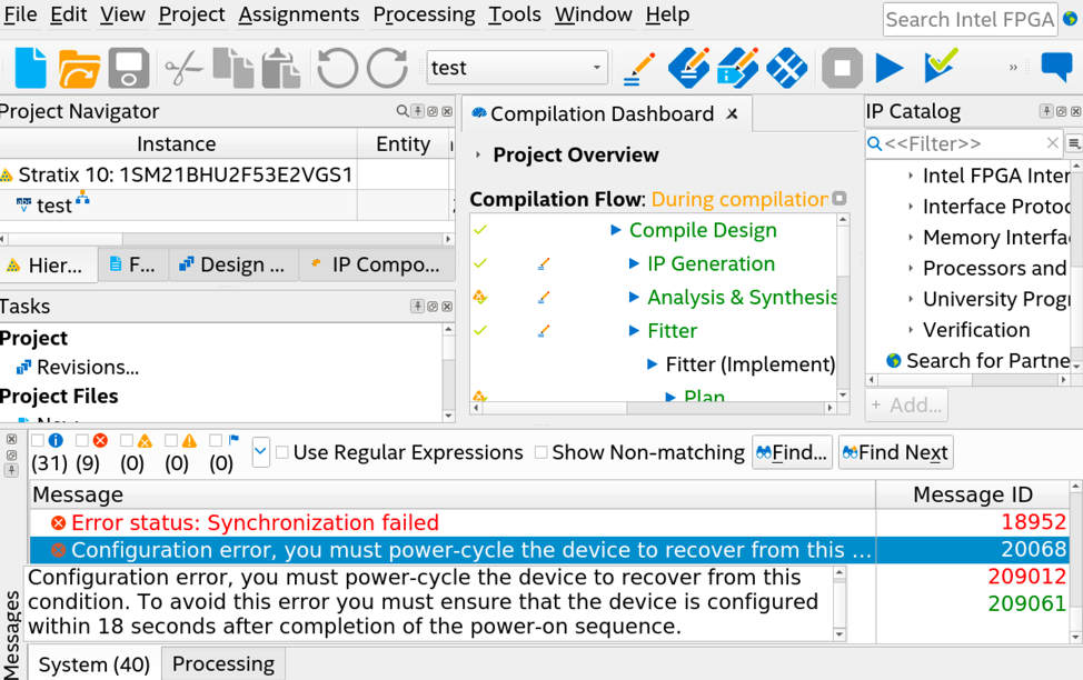
I was trying to download the bitstream through the J15 port using a programming cable. However, I got the error message saying "Synchronization failed. Configuration error." The following figure shows more information about the error:
I do the following things for programming the board:
(1) Create a new project for my device (1SM21BHU2F53E2VGS1), write a simple 4-bit counter in Verilog and generate the bitstream (test.sof).
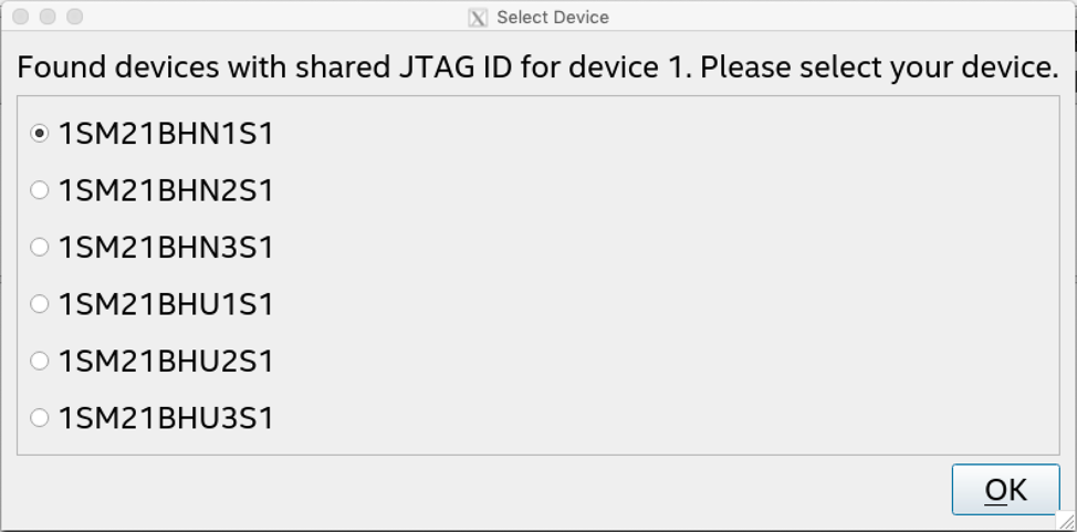
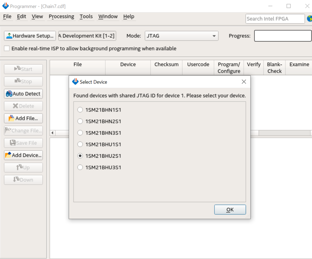
(2) Open the "Programmer" and press the "Auto Detect". Then I have to choose the device with following options:
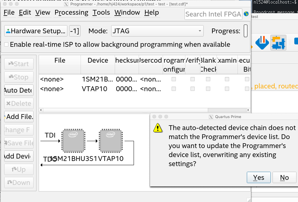
However, no one exactly matches to my board (1SM21BHU2F53E2VGS1). Thus I simply try the last three options which seems highly related to my board, but I get the following critical warning:
(3) After clicking "Yes", I select the device (named with "1SM21BXXX") and click "Change File"; in the pop-up window, I select the bitstream generated in step (1), i.e., test.sof
(4) Finally I press the "Start" button to program the board and get the error mentioned before ("Synchronization failed. Configuration error." ).
Anyone knows what I'm doing wrong here? Any response will be greatly appreciated!
Thanks,
Hanchen
Link Copied
- Mark as New
- Bookmark
- Subscribe
- Mute
- Subscribe to RSS Feed
- Permalink
- Report Inappropriate Content
Hi,
May I know if you can directly program the FPGA when you start powering up your PC?
- Mark as New
- Bookmark
- Subscribe
- Mute
- Subscribe to RSS Feed
- Permalink
- Report Inappropriate Content
Thanks for your reply!
No, I can't. What I tried before is directly programming the FPGA through the JTAG port (J15 on the Stratix 10 MX board). And I got the error saying "Synchronization failed. Configuration error" (The figure I attached in my original post shows more detail about the error message).
- Mark as New
- Bookmark
- Subscribe
- Mute
- Subscribe to RSS Feed
- Permalink
- Report Inappropriate Content
Hi,
May I know if you are observing it during the starting of powering the board? May I know if you facing the same issue when you remove the board from the system and power on the board using the external power supply?
- Mark as New
- Bookmark
- Subscribe
- Mute
- Subscribe to RSS Feed
- Permalink
- Report Inappropriate Content
Hi,
Please refer the workaround and fixed in https://www.intel.com/content/altera-www/global/en_us/index/support/support-resources/knowledge-base/component/2018/why-does-my-stratix10-device-fail-to-configure-if-there-is-a-del.html to resolved your issue.
- Mark as New
- Bookmark
- Subscribe
- Mute
- Subscribe to RSS Feed
- Permalink
- Report Inappropriate Content
Thank you so much for your reply. But after patching my Quartus 18.0, I'm still getting the same error mentioned before. Any other suggestions I can try to resolve this error?
Also, I'm curious about the following step:
(2) Open the "Programmer" and press the "Auto Detect". Then I have to choose the device with following options:
The problem is that no available option exactly matches my board (1SM21BHU2F53E2VGS1). Could this leading to the downloading error?
Thanks,
Hanchen
- Mark as New
- Bookmark
- Subscribe
- Mute
- Subscribe to RSS Feed
- Permalink
- Report Inappropriate Content
Hi,
Your device should be 1SM21BHU2S1. May I know if you use external power supply to power on the board then can you programmed it immediately after power on?
- Mark as New
- Bookmark
- Subscribe
- Mute
- Subscribe to RSS Feed
- Permalink
- Report Inappropriate Content
Thanks for your reply!
No, I can't. But when using the external power supply, I got different error messages:
(18948) Error message received from device: Detected hardware access error. There is a failure in accessing external hardware. (Subcode 0x0032, Info 0x00000000, Location 0x0000B800)
(20072) A PMBUS error has occurred during configuration. Potential errors: incorrect VID setting in Quartus Project. The target device fails to communicate to smart regulator or PMBUS Master on board.
(209012) Operation failed.
After searching online, I find the following solution to this error:
https://www.intel.com/content/www/us/en/programmable/support/support-resources/knowledge-base/component/2017/error-18948---error-message-received-from-device--detected-inval.html
It seems that I have to configure the DIP switches to the JTAG only mode. Thus I change the DIP switches to the following configuration:
SW2[3:0] = 1111, SW1[3:0] = 1111;
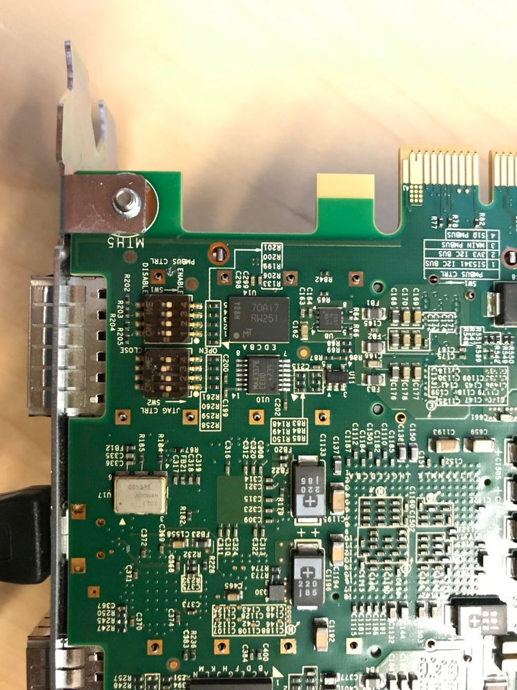
According to the user guide of Stratix 10 MX (https://www.intel.com/content/www/us/en/programmable/documentation/cbc1517362051825.html#sgk1519171036412), I changed the SW2 to set up the JTAG only mode, as shown in the following picture:
However, with this DIP switching configuration, I got the message "Unable to scan device chain. Can't scan JTAG chain. Do you want to open the JTAG Chain Debugger to troubleshoot the JTAG chain?" I guess this error is caused by the wrong setting of DIP switches. A picture of the correct DIP switch setting for the JTAG only mode will be greatly appreciated.
Thanks,
Hanchen
- Mark as New
- Bookmark
- Subscribe
- Mute
- Subscribe to RSS Feed
- Permalink
- Report Inappropriate Content
Hi,
May I know if you are able to share with me your sof file?
- Mark as New
- Bookmark
- Subscribe
- Mute
- Subscribe to RSS Feed
- Permalink
- Report Inappropriate Content
Sure. This sof file is generated by Quartus Prime Pro 18.0 patched with patch 0.13 Linux provided in the following link:
https://www.intel.com/content/altera-www/global/en_us/index/support/support-resources/knowledge-base/component/2018/why-does-my-stratix10-device-fail-to-configure-if-there-is-a-del.html
- Mark as New
- Bookmark
- Subscribe
- Mute
- Subscribe to RSS Feed
- Permalink
- Report Inappropriate Content
- Mark as New
- Bookmark
- Subscribe
- Mute
- Subscribe to RSS Feed
- Permalink
- Report Inappropriate Content
Thanks for your help. I just tried your sof file with the JTAG only mode configuration:
SW2[3:0] = 1111, SW1[3:0] = 1111;
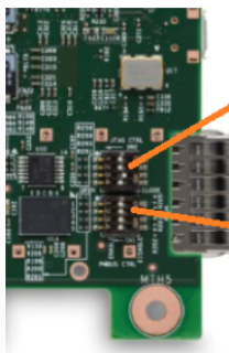
As I showed before, the following picture is my setting of DIP switches:
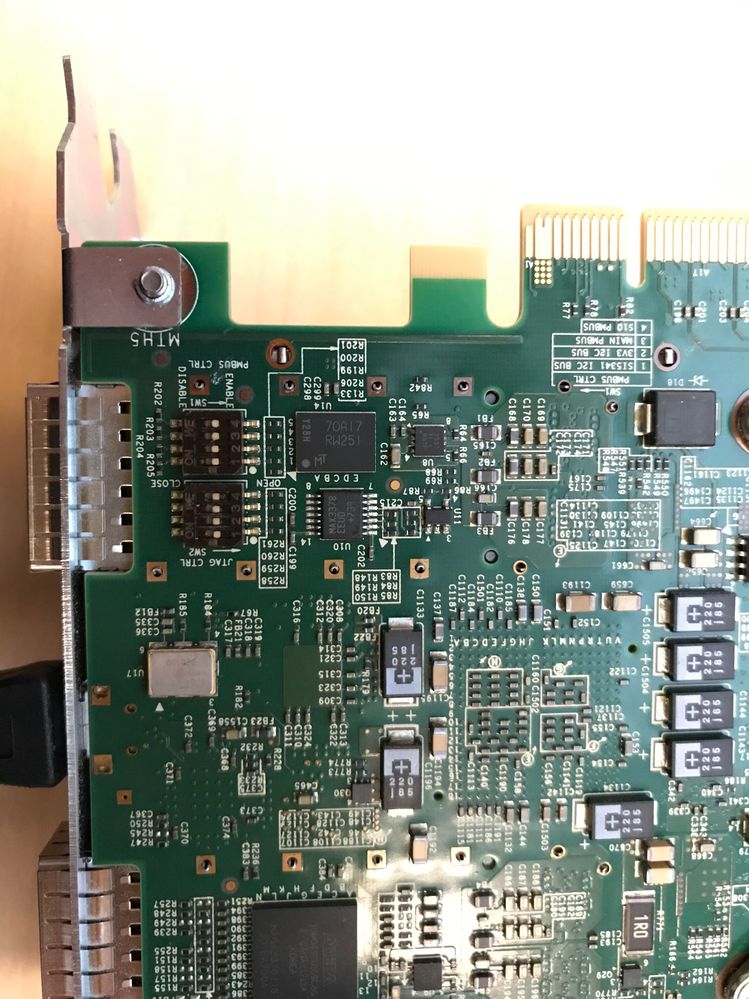
As I posted before, I suspected that my DIP switch configuration was wrong so that the synchronization between PC and s10mx board cannot be correctly established. Thus, I tried the default DIP switch setting in the following documentation:
https://www.intel.com/content/www/us/en/programmable/documentation/cbc1517362051825.html#sgk1519171036412
Surprisingly, by using that default DIP switch setting, I can successfully download both your sof file (bts_pcie.sof) and my own test sof file (test.sof) to the s10mx board. However, I still have some questions about the unexpected success. But before that, let me first share my configuration of successful downloading the bitstream to the s10 mx board.
(1) Change the DIP switch back to the default setting:
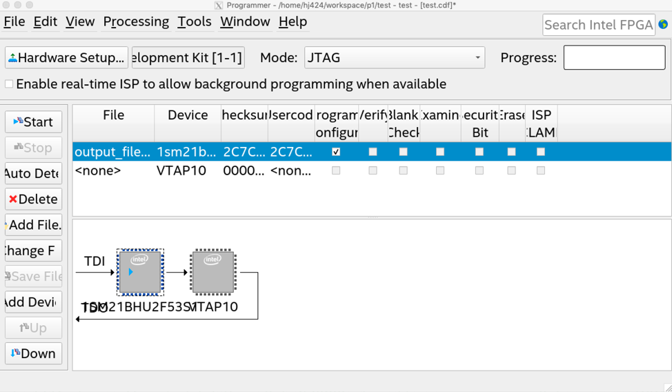
(2) Open the Quartus Programmer, press "Auto Detect" and select the correct JTAG ID for device 1 (1SM21BHU2F53E2VGS1). We should choose "1SM21BHU2S1" for my s10mx board.
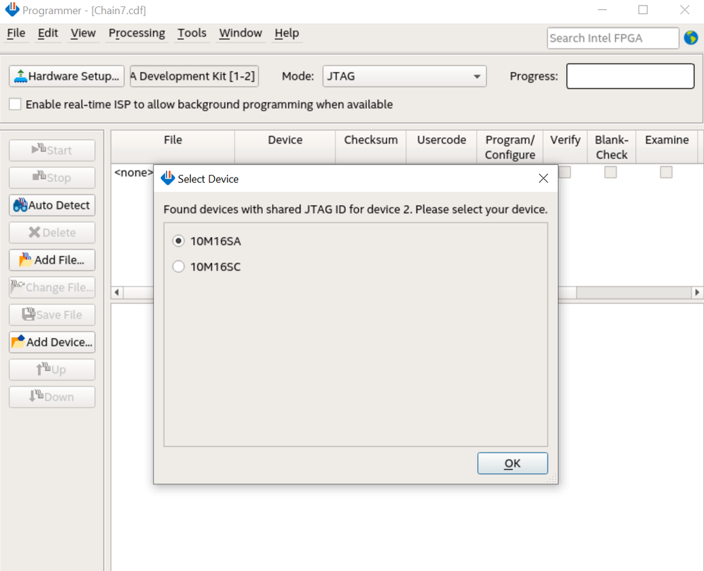
(2) Choose the correct JTAG ID for device 2. I think the device 2 means the Intel MAM 10 FPGA Power Manager, so I choose "10M16SA" for my board according to the s10 mx user guide:
https://www.intel.com/content/www/us/en/programmable/documentation/cbc1517362051825.html#sgk1519171036412
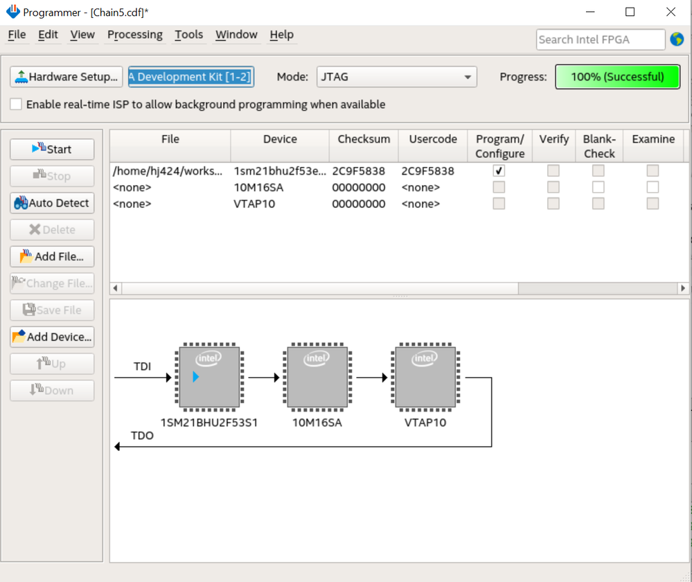
(3) Replace the device (1SM21BHU2F53S1) with the bitstream (sof file). And click "Start", the bitstream was successfully downloaded to the board.
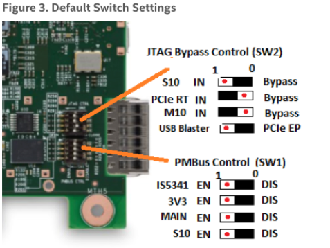
However, I'm confused of the following figure from s10mx user guide:
There is a mismatch between the real board and the explanation in terms of the PCIe RT signal. In specific, the PCIe RT setting in the real board was set to the left side. But the PCIe RT setting in the explanation was set to the right side. So my first question is:
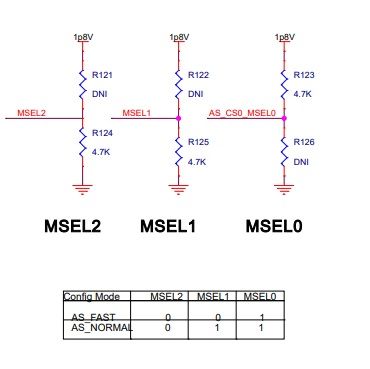
(1) What is the corresponding MSEL[2:0] for the real board setting in Figure 3?
Then my second question is:
(2) According to the s10 mx user guide, s10mx supports AS mode (MSEL[2:0] = 001) and JTAG mode (MSEL = 111). I assume the default setting shown in Figure 3 means AS mode and adjust my DIP switches to JTAG mode. But when downloading bitstream in the JTAG mode, I got the error message "Unable to scan device chain. Can't scan JTAG chain. Do you want to open the JTAG Chain Debugger to troubleshoot the JTAG chain?" What is the problem here? I'm not sure what is the correct DIP switch configuration for the JTAG mode (MSEL = 111). A picture of that JTAG configuration will be greatly appreciated.
Thanks,
Hanchen
- Mark as New
- Bookmark
- Subscribe
- Mute
- Subscribe to RSS Feed
- Permalink
- Report Inappropriate Content
Hi,
The board does not support MSEL changes using DIP Switches. In order to make the changes in MSEL then you need to modify the Weak-pull up and weak pull down of the resistor on the board.
- Mark as New
- Bookmark
- Subscribe
- Mute
- Subscribe to RSS Feed
- Permalink
- Report Inappropriate Content
- Mark as New
- Bookmark
- Subscribe
- Mute
- Subscribe to RSS Feed
- Permalink
- Report Inappropriate Content
I see. Thank you so much for the clarification!
But I'm still confused with the inconsistency of DIP switches configuration in the documentation. For example, in the following Figure 3, there is a mismatch between the real board and the explanation in terms of the PCIe RT signal. In specific, the PCIe RT setting in the real board was set to the left side. But the PCIe RT setting in the explanation was set to the right side.
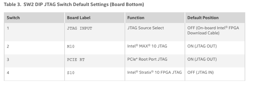
Also, from Figure 3, it seems like SW2-1 corresponds to the board label named "S10". However, the board label named "S10" is actually SW2-4 in Table 3.
Thus I have the following two questions:
(1) What is the real position of "S10"? SW2-1 or SW2-4?
(2) What is the correct explanation of the default setting of SW2?
Thanks,
Hanchen
- Mark as New
- Bookmark
- Subscribe
- Mute
- Subscribe to RSS Feed
- Permalink
- Report Inappropriate Content
Hi,
1) The position and explanation of the SW2 is correct. The direction is from bottom to top. SW2-1 is JTAG Input, SW2-2 is M10, SW2-3 is PCIe RT, SW2-4 is S10.
2) The correct default setting is based on the Table 3 or the expanded switch. Please do not follow the exact board switch setting.
- Subscribe to RSS Feed
- Mark Topic as New
- Mark Topic as Read
- Float this Topic for Current User
- Bookmark
- Subscribe
- Printer Friendly Page
