- Mark as New
- Bookmark
- Subscribe
- Mute
- Subscribe to RSS Feed
- Permalink
- Report Inappropriate Content
Hello, I just feel strange with AN477 doc below:
https://www.intel.com/content/dam/www/programmable/us/en/pdfs/literature/an/an477.pdf
page 12
why the
Calculated output maximum delay = tsu of external register = –0.9 ns
is not -tsu of external register ?
or = 0.9 ns ?
thanks for your help
- Mark as New
- Bookmark
- Subscribe
- Mute
- Subscribe to RSS Feed
- Permalink
- Report Inappropriate Content
This is because
1) The multicycle assignments are used to create a setup relationship of 0ns and a hold relationship of -1/2*period.
2) The value for set_output_delay -max is now negative due to the 0ns setup relationship set by the multicycle then the setup requirement (max data delay).
Link Copied
- Mark as New
- Bookmark
- Subscribe
- Mute
- Subscribe to RSS Feed
- Permalink
- Report Inappropriate Content
This is because
1) The multicycle assignments are used to create a setup relationship of 0ns and a hold relationship of -1/2*period.
2) The value for set_output_delay -max is now negative due to the 0ns setup relationship set by the multicycle then the setup requirement (max data delay).
- Mark as New
- Bookmark
- Subscribe
- Mute
- Subscribe to RSS Feed
- Permalink
- Report Inappropriate Content
- Mark as New
- Bookmark
- Subscribe
- Mute
- Subscribe to RSS Feed
- Permalink
- Report Inappropriate Content
Sorry,
I have thought for a long time, but I still don't understand. Could you describe it in detail? thank you
- Mark as New
- Bookmark
- Subscribe
- Mute
- Subscribe to RSS Feed
- Permalink
- Report Inappropriate Content
may be https://www.intel.com/content/dam/www/programmable/us/en/pdfs/literature/an/an411.pdf page 32 can help?
- Mark as New
- Bookmark
- Subscribe
- Mute
- Subscribe to RSS Feed
- Permalink
- Report Inappropriate Content
Any update?
- Mark as New
- Bookmark
- Subscribe
- Mute
- Subscribe to RSS Feed
- Permalink
- Report Inappropriate Content
For personal reasons, I'm sorry to reply you so late.
For AN411,I have read page 32.
I can understand why Multicycle set , for same edge launch and latch. I don't understand why max data delay now is negative.
Q1:
i don't understand max data delay is negative has some related to Multicycle. and why data delay is negative.
Q2:
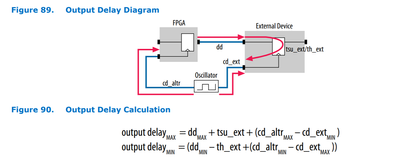
Is it analyzed according to this formula?
I'm sorry for the trouble!
Have a good day.
- Subscribe to RSS Feed
- Mark Topic as New
- Mark Topic as Read
- Float this Topic for Current User
- Bookmark
- Subscribe
- Printer Friendly Page

