- Mark as New
- Bookmark
- Subscribe
- Mute
- Subscribe to RSS Feed
- Permalink
- Report Inappropriate Content
Hi, we are using 10AX057H3F34E2SG for PCIe GEN3.0 x4 lanes, connected to a PC module by Board to Board connects.
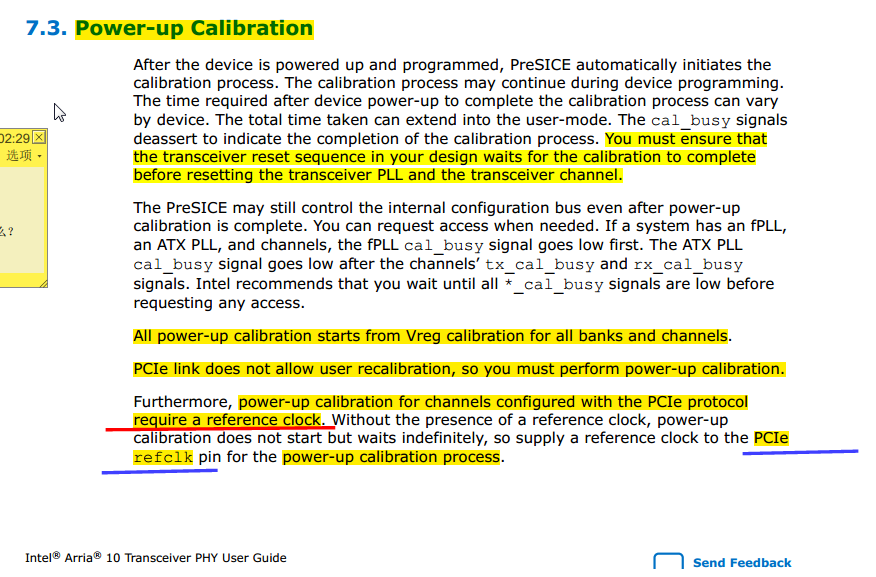
I read on section 7.3 of UG-01143 (Arria 10 Transceiver PHY User Guide, page582) that user need to provide a CLOCK for proper transceiver for power-up calibration, and only Power-ON Calibration are allowed for PCIe..
Question1: Is this CLK refer to CLKUSR or dedicated XCVR REFCLK pin pairs, or both? As marked with red and blue lines in below picture. I guess both CLKUSR and XCVR clock should be provided to FPGA. But still need intel confirm.
", and may extend into user-mode.
How to understand this? I guess the seuqence should be Power on -->Configuration-->Initialization-->XCVR Calinration( user mode in parallel). Not sure......When EXACTLY the calibration begins? Is there timing diagrams on Intel docs?
Question3: To avoid the well-known “100 ms boot time requirement for PCIe”, We decide to power FPGA first, after detect the CONFIG_DONE signal be pulled high, then start PC, then the PCIe reference clock will be sent from PC to FPGA GXB banks.
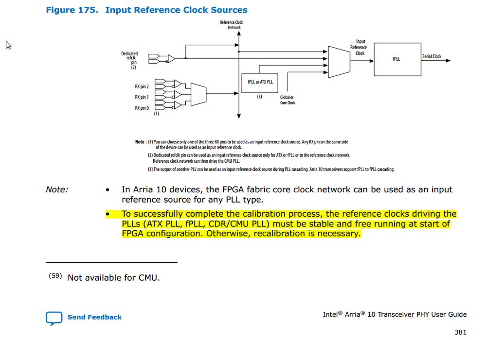
However, this will be CONFLICT with UG-01143 section 3.2 , page381 note, which writes “To successfully complete the calibration process, the reference clocks driving the PLLs (ATX PLL, fPLL, CDR/CMU PLL) must be stable and free running at start of FPGA configuration”. Do you have any insight about how could we solve this conflict?
For now, we use ASx4 config scheme, and no likely to change it for other config schemes.
Thanks very much!
- Tags:
- PERST
- Mark as New
- Bookmark
- Subscribe
- Mute
- Subscribe to RSS Feed
- Permalink
- Report Inappropriate Content
Hi @xytech
Calibration starts during configuration.
No timing sequence, the time for calibration to complete vary by device.
Based on experience, faster configuration time is needed if you are designing for open-system to meet the 100ms. For closed-system, you can adjust the PERST to allow more time.
Hope this helps.
Link Copied
- Mark as New
- Bookmark
- Subscribe
- Mute
- Subscribe to RSS Feed
- Permalink
- Report Inappropriate Content
- Mark as New
- Bookmark
- Subscribe
- Mute
- Subscribe to RSS Feed
- Permalink
- Report Inappropriate Content
anyone could help one this topic? Thanks.
- Mark as New
- Bookmark
- Subscribe
- Mute
- Subscribe to RSS Feed
- Permalink
- Report Inappropriate Content
up
- Mark as New
- Bookmark
- Subscribe
- Mute
- Subscribe to RSS Feed
- Permalink
- Report Inappropriate Content
copy from other post. reocorded here.
The total configuration timing sequence is;
1) External power gets turned on to the "system"; motherboard or chassis, main host CPU, and PCIe bridges and devices.
2) The power supplies for the host and the peripheral devices start ramping up. The timing for this part is completely arbitrary and depends on the system design. In the case of your FPGA-based PCIe end-point, you'll have whatever ramp time your power supplies require, and if you've specified a fast POR, they need to ramp within that time.
3) Once the power supplies are in spec, the FPGA configures, eg., via Active Serial, Passive Serial, or Fast Passive Parallel.
4) The BIOS or host CPU bootloader enumerates the PCIe bus. So long as (3) completes before (4), your system will work, otherwise it will not, as the PCIe device will not be enumerated.
- Mark as New
- Bookmark
- Subscribe
- Mute
- Subscribe to RSS Feed
- Permalink
- Report Inappropriate Content
.
- Mark as New
- Bookmark
- Subscribe
- Mute
- Subscribe to RSS Feed
- Permalink
- Report Inappropriate Content
up
- Mark as New
- Bookmark
- Subscribe
- Mute
- Subscribe to RSS Feed
- Permalink
- Report Inappropriate Content
up
- Mark as New
- Bookmark
- Subscribe
- Mute
- Subscribe to RSS Feed
- Permalink
- Report Inappropriate Content
UP
- Mark as New
- Bookmark
- Subscribe
- Mute
- Subscribe to RSS Feed
- Permalink
- Report Inappropriate Content
Hi @xytech,
Let me try to help out here.
Q1: Yes, both.
Q2: Calibration starts as soon as FPGA is powered. Cal_busy goes low to indicate calibration completion.
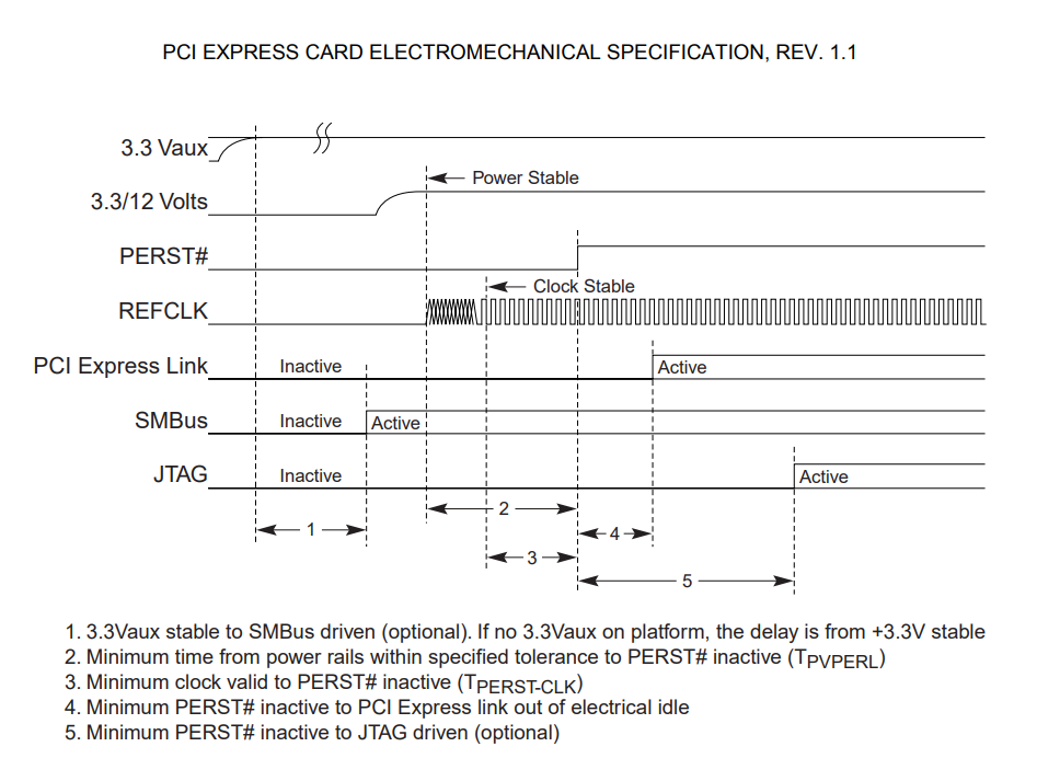
Q3: The 100Mhz refclk for PCIe must be stable before FPGA is powered. See diagram of PCIe spec, FPGA should configuration within point (3). Link training is somewhere within (4).
Hope this helps.
- Mark as New
- Bookmark
- Subscribe
- Mute
- Subscribe to RSS Feed
- Permalink
- Report Inappropriate Content
Hi JwChin, thank you very much for patient reply.
For Q2, As you mentioned “Calibration starts as soon as FPGA is powered”. Is it start AFTER or parallel with Configuration Starting Moment? This confusion came from between First and Second sentences on page582 section7.3 of ug-01143 ( as pic in my original post). And Is there some Intel document describes the timing sequence of related signals ?
According to you information, it seems that we have no choice but to change our config scheme from ASx4 to FPP for faster configuration time. Or we might use Partial Reconfiguration or Configuration Data Compression, but it will consume more work for our FPGA staffs.
Thanks again, and look forwar to your discussion.
- Mark as New
- Bookmark
- Subscribe
- Mute
- Subscribe to RSS Feed
- Permalink
- Report Inappropriate Content
Hi @xytech,
There are two main types of calibration.
• Power-up calibration—Initiates automatically at device power-up and runs during device configuration.
• User calibration—If you perform dynamic reconfiguration or change the reference clock frequency of the I/O PLL, you must perform user recalibration. You must enable the required calibration sequence.
With that, answer to "Is it start AFTER or parallel with Configuration Starting Moment?" should be parallel with the configuration process.
There is no timing sequence for the calibration process as the time required after device power-up to complete the calibration process can vary by device. That's why you will need the cal_busy signal to know when it completes.
Just my 2 cents, as to ASx4 to FPP, I think it depends the PCIe is used for open-system (need to meet 100ms requirement) or closed-system (up to you to decide). If it is a closed-system, I dont see why you need to change to FPP, you can delay the #PERST to allow more time.
I hope this helps.
- Mark as New
- Bookmark
- Subscribe
- Mute
- Subscribe to RSS Feed
- Permalink
- Report Inappropriate Content
Hi @xytech
Calibration starts during configuration.
No timing sequence, the time for calibration to complete vary by device.
Based on experience, faster configuration time is needed if you are designing for open-system to meet the 100ms. For closed-system, you can adjust the PERST to allow more time.
Hope this helps.
- Mark as New
- Bookmark
- Subscribe
- Mute
- Subscribe to RSS Feed
- Permalink
- Report Inappropriate Content
Hi JwChin, thank you very much for patient reply.
As UG-01143 section 7.3 writes, PCIe links do not allow user recalibration. We have no choice. Only can do power up calibration.
OK, finally confirmed that Calibration starts during configuration and no specific timing, cal_busy indicates Calibration completes.
Yes, we do design OPEN-System. Root PCIe node is a standard x86 COMe module (compact PC module), and we cannot control when PERST# will be released.
Actually in our older product, we use Artix-7A200T FPGA of Xilinx, which DO NOT explicitly requires “transceiver Reference clock must be stable and free running BEFORE FPGA powered up for successful XCVR calib”(they do not need CLKUSR neither) , so our system are designed to power FPGA first, after detect its CONFIG_DONE signal released (pulled high), then we start PC module, this made sure PC can enumerate FPGA PCIe node. It worked fine.
Now it’s clear that this solution is NOT suitable for Intel A10. So we must change a fast enough configuration scheme to satisfy PCIe 100ms requirement. Hardware and/or Logic design need modifications inevitablely.
Thanks again for your kind help. Good day
- Mark as New
- Bookmark
- Subscribe
- Mute
- Subscribe to RSS Feed
- Permalink
- Report Inappropriate Content
With an Arria 10 design at that density, I would recommend looking at CvP (configuration via protocol). My understanding is that this is meant to load the periphery of FPGA (including PCIe core) in order to satisfy the 100ms enumeration requirement. Then the "core" FPGA (rest of the logic) is loaded after the PCIe interface is safely up. Looks like datasheet calls out minimum config time for that device of >600ms when using AS (active serial) x4. Best case for FPP is slightly less than 100ms.
Regarding calibration, both clocks should be required (PCI_REFCLK and CLKUSR). CLKUSR toggles PreSICE state machine that runs the calibrations and you need the REFCLK for the PLLs. Keep in mind that in A10 devices, PCIe (w/ hard IP) are the first devices that calibrate and then cascade the CAL* status bits downstream to other GXBs on the chip. If you have a PCIe interface instantiated in your project that's not hooked up to anything (so not successfully calibrating), it will gate other GXBs from calibrating. Running into that right now with a design.
- Mark as New
- Bookmark
- Subscribe
- Mute
- Subscribe to RSS Feed
- Permalink
- Report Inappropriate Content
Hi JCann,
Thanks for reply. We use 2 GXB banks for PCIe GEN3.0 x8 linked to a Standard PC module. The rest 2 GXB banks are used for communication between two Arial 10 FPGAs.
Just to confirm I percept your second paragraph correctly, is following what you mean?
------After FPGA is powered up, among all GXBs, PCIe hard IP GXBs are firstly calibrated, and then certain CAL* status bits/signals are cascaded (delivered) downstream to other 2 GXBs for calibrating. If PCIe GXBs is not successfully calibrated, it will GATE(Prevent) other GXBs from calibrating, which means finally all GXB banks will not be calibrated successfully , and cannot function correctly. ------
Furthermore, as UG-01143 writes, “Transceivers include both analog and digital blocks that require calibration to compensate for process, voltage, and temperature (PVT) variations”
Just wondering, if it’s not calibrated successfully, how will transceivers behave? Will it become unable to work completely, or work with de-rated performance, such as lower speed rate, worse BER?
And if we enable datas compression funtion in Quartus to reduce bits stream file's size(typically reduce by 30%-55%), will the config time be reduced?
Thanks for helping!
- Mark as New
- Bookmark
- Subscribe
- Mute
- Subscribe to RSS Feed
- Permalink
- Report Inappropriate Content
Given your specific implementation - my understanding of how A10 GXBs work (with PCIe) is that both of the PCIe banks need to be connected to a host and properly calibrated in order for the 2x GXBs that are used for inter-FPGA communication can be properly calibrated. This is assuming that both PCIe Gen3x8 are using the Hard IP (HIP). Rules might be different if not using HIP, but I would guess that you went the route of HIP for this device. The use case that I have is using another piece of DisplayPort IP that has calibration logic built into it. I can't speak to whether you would expect de-rated performance on a link where you have control over PLL+reconfig+PHY and could possibly "trick" it into thinking that it's OK based on lack of calibration (not recommended).
I just wanted to point out that there are some interesting dependencies that need to be accounted for when using PCIe HIP that might or might not be connected.
- Mark as New
- Bookmark
- Subscribe
- Mute
- Subscribe to RSS Feed
- Permalink
- Report Inappropriate Content
Hi JCann,
We found solution for this pcie 100ms problem. In <ug01145_a10_pcie_avmm> doc, it clearly states that "Autonomous Mode" can satisfy pcie 100ms wake up time as long as user choose the specific hard pcie IP. this info is on section 12.2.
https://www.intel.com/content/dam/www/programmable/us/en/pdfs/literature/ug/ug_a10_pcie_avmm.pdf
thanks again for help. good day.
- Subscribe to RSS Feed
- Mark Topic as New
- Mark Topic as Read
- Float this Topic for Current User
- Bookmark
- Subscribe
- Printer Friendly Page

