- Mark as New
- Bookmark
- Subscribe
- Mute
- Subscribe to RSS Feed
- Permalink
- Report Inappropriate Content
Trying to configure a Cyclone V 5CEFA2U19I7 with an MX25L256 fails. The device is MX25L25645GZ2I-08G. It is configured to use Active Serial x4. Here is more information.
- Programming .SOF through JTAG works fine.
- We can create and program the MX25L256 with a .JIC file.
- The Examine reads back the same data that is programmed with the JIC.
- We have tried Active Serial x1 and Active Serial X4.
- We have tried AS Fast and AS Standard.
- We have tried Quartus Lite 20.1.1.720 and 21.1.0.842.
- We have tried the Internal Oscillator at 100 MHz and at 12.5MHz.
The behavior is the same. After power on, the FPGA reads the SPI FLASH. After the read is complete, the DCLK changes to the configuration clock frequency. Before configuration completes, nSTATUS goes low and the FPGA re-starts configuration. All power rails look good.
Link Copied
- Mark as New
- Bookmark
- Subscribe
- Mute
- Subscribe to RSS Feed
- Permalink
- Report Inappropriate Content
Hi,
I am Farabi who will support your configuration issue.
The nSTATUS goes low during configuration means some setting is not set the correct way.
May I know how you connect the MSEL pins? are they connected to some other controller IOs or are they connected to a fixed connection like pull high/pull low (by switches)?
regards,
Farabi
- Mark as New
- Bookmark
- Subscribe
- Mute
- Subscribe to RSS Feed
- Permalink
- Report Inappropriate Content
Hello,
Do you have any updates? Or you can private email me the schematic of configuration connection page.
regards,
Farabi
- Mark as New
- Bookmark
- Subscribe
- Mute
- Subscribe to RSS Feed
- Permalink
- Report Inappropriate Content
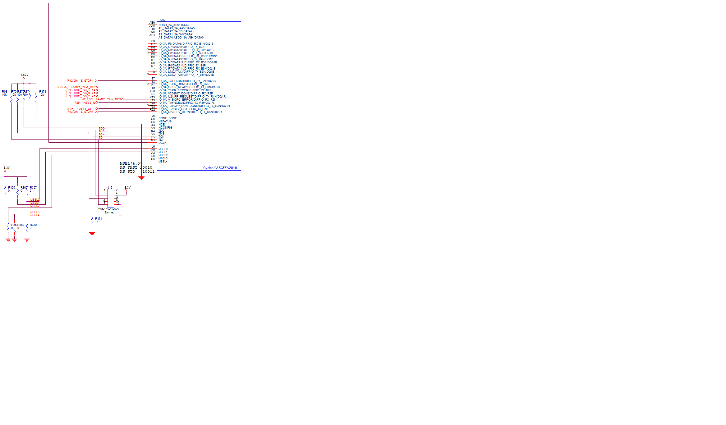
The MSEL pins are connected through zero Ohm resistors. We have tried AS Standard (R370 out and R367 in) and AS Fast(R370 in and R367 out) . I have attached a picture.
- Mark as New
- Bookmark
- Subscribe
- Mute
- Subscribe to RSS Feed
- Permalink
- Report Inappropriate Content
Do you need a copy of the .JIC file? We have created one with all combinations of the Advanced options and all behave the same.
Disable EPCS/EPCQ ID check
Disable AS mode CONF_DONE error check.
- Mark as New
- Bookmark
- Subscribe
- Mute
- Subscribe to RSS Feed
- Permalink
- Report Inappropriate Content
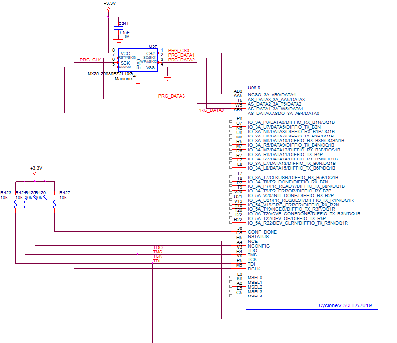
I have attached a picture with the connections to the SPI FLASH
- Mark as New
- Bookmark
- Subscribe
- Mute
- Subscribe to RSS Feed
- Permalink
- Report Inappropriate Content
More information.
I have created a custom device to try different settings. Can you get me information about how the programmer sets up the FLASH and the commands that the Cyclone V issues to configure the FPGA.
We tried an ASx1 JIC file and looked at the transactions. The FPGA issued a RDSR (Read Status Register) command and read back 0x40. This indicates that QUAD ENABLE bit is set. This was supposed to be an ASx1 file so I thought that the programmer would have cleared that bit. The FPGA also issues a RDID which returns the expected data. After that, the FPGA reads data and tries to configure. The DCLK changes frequency but the configuration fails.
Does the programmer set values in non-volatile memory in the FPGA to configure the type of SPI FLASH? What should the programming sequence be? I noticed the defaults in the custom device set 4 byte addressing and then turn it off under termination. When we monitored the configuration sequence, we never see 4 byte addressing get enabled.
- Mark as New
- Bookmark
- Subscribe
- Mute
- Subscribe to RSS Feed
- Permalink
- Report Inappropriate Content
Hi,
I am referring to this link: https://www.intel.com/content/www/us/en/docs/programmable/683271/current/understanding-quad-spi-flash-byte-addressing.html
there is dummy cycle that is required. for 4-byte addressing, 4 dummy cycles is required before the config block controller receiving the valid bitstream.

and I compare with Macronix handbook below, it needs to set DC0 and DC1 accordingly in the configuration register.

and then I compare to AS configuration timing diagram, FGPA need to supply DCLK signal until all bits completely transferred to FPGA.

regards,
Farabi
- Mark as New
- Bookmark
- Subscribe
- Mute
- Subscribe to RSS Feed
- Permalink
- Report Inappropriate Content
- Mark as New
- Bookmark
- Subscribe
- Mute
- Subscribe to RSS Feed
- Permalink
- Report Inappropriate Content
Hello,
Do you have further question?
regards,
Farabi
- Mark as New
- Bookmark
- Subscribe
- Mute
- Subscribe to RSS Feed
- Permalink
- Report Inappropriate Content
Hi,
We do not receive any response from you to the previous question/reply/answer that I have provided. This thread will be transitioned to community support. If you have a new question, feel free to open a new thread to get the support from Intel experts. Otherwise, the community users will continue to help you on this thread. Thank you.
regards,
Farabi
- Subscribe to RSS Feed
- Mark Topic as New
- Mark Topic as Read
- Float this Topic for Current User
- Bookmark
- Subscribe
- Printer Friendly Page