- Mark as New
- Bookmark
- Subscribe
- Mute
- Subscribe to RSS Feed
- Permalink
- Report Inappropriate Content
Hello,
i want to use 2GByte DDR3 Memory (2x16 Bit Chips)
Does it make any difference if using Bank 3A/3B instead of Bank 2K/2J?
In Quartus In Planner Pins of BANK 2K/2J are marked as "Hard Processor System Pin". What dies this exactly mean?
Thanks very much!
Link Copied
- Mark as New
- Bookmark
- Subscribe
- Mute
- Subscribe to RSS Feed
- Permalink
- Report Inappropriate Content
Hi Sir,
For any given EMIF configuration, the pin-out of the EMIF-to-HPS interface is fixed. Banks and pins used for HPS access to a DDR interface are labeled HPS_DDR in the HPS Function column of the pin-out file. By default, the Intel FPGA that supported EMIF for HPS IP core together with the Intel Quartus Prime Fitter automatically implement the correct pin-out for HPS EMIF without user having to implement additional constraints. The supported Intel FPGA for HPS included Stratix 10 , Arria 10 , Agilex and etc.
Unfortunately, HPS is not supported for Cyclone 10 GX. So, you can freely use both I/O column 2 (Bank 2K/2J) and I/O column 3 (Bank 3A/3B) for EMIF placement. There is no difference in placing EMIF into both I/O column.
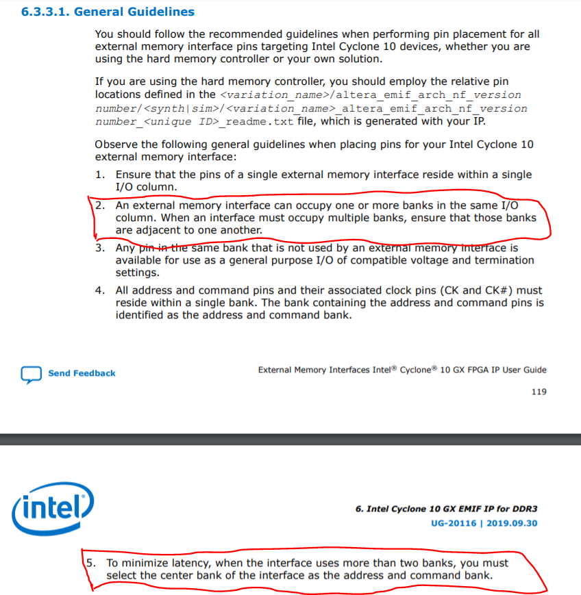
For more info, you can refer to section "6.3.3. Pin Guidelines for Intel Cyclone 10 GX EMIF IP" and section "6.3.3.1. General Guidelines" of this UG. It mentioned about certain requirements when placing the EMIF pins --> https://www.intel.com/content/dam/www/programmable/us/en/pdfs/literature/ug/ug-20116.pdf
Hope this helps.
Thanks
Regards,
Aida
- Mark as New
- Bookmark
- Subscribe
- Mute
- Subscribe to RSS Feed
- Permalink
- Report Inappropriate Content
Hello,
thank you very much for your answer!
Can this also be mixed. So for example using Bank 3B for Address/Command Lines and using Bank 2K for Data Lines?
BR,
Roland
- Mark as New
- Bookmark
- Subscribe
- Mute
- Subscribe to RSS Feed
- Permalink
- Report Inappropriate Content
Hi Sir,
No, it can't be mixed. When an interface used multiple banks, those banks need to be adjacent to one another as mentioned in the UG link shared previously.
For example, a physical pin with a Bank Number of 2K and Index within I/O Bank of 22, indicates that the pin resides in I/O lane 2, in I/O bank 2K, in column 2. The adjacent I/O banks are 2J and 2L.
You can always assume I/O banks are adjacent within an I/O column except in the following conditions:
- When an I/O bank is not bonded out on the package (contains the '-' symbol in the I/O table).
- An I/O bank does not contain 48 pins, indicating it is only partially bonded out.
- The pairing pin for an I/O pin is located in the same I/O bank. You can identify the pairing pin by adding one to its Index within I/O Bank number (if it is an even number), or by subtracting one from its Index within I/O Bank number (if it is an odd number).
For address/command pins, it is recommended to place it at the center banks to minimize latency. For example, interface that required total of 3 I/O banks (Bank 3A,3B and 3C). The pins placement is recommended as below:
Bank 3A : Data pins
Bank 3B: Address/Command
Bank 3C: Data pins
Regards,
Aida
- Subscribe to RSS Feed
- Mark Topic as New
- Mark Topic as Read
- Float this Topic for Current User
- Bookmark
- Subscribe
- Printer Friendly Page
