- Mark as New
- Bookmark
- Subscribe
- Mute
- Subscribe to RSS Feed
- Permalink
- Report Inappropriate Content
Hi,
I instantiate a EMIF IP core with DDR4 protocol in my design, modify memory timing parameters and board skew values.
The DDR4 speed bin is 2400 and CL=16.
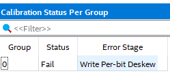
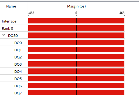
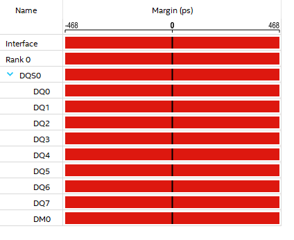
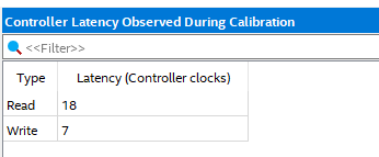
After programming the device in EMIF debug toolkit, I get the following calibration report, and emif_clk_user is correct, measured 267MHz≈1066.667MHz/4, but the local_cal_sucess is low.
The following pictures and txt files are resluts of EMIF debug toolkit. I will be appreciated if anyone can give me some suggestions.
Thanks, regards.
Link Copied
- Mark as New
- Bookmark
- Subscribe
- Mute
- Subscribe to RSS Feed
- Permalink
- Report Inappropriate Content
Hi, I assume this is on your custom board? do you have the RZQ resistor connect on board?
Also, here is the checklist that you can refer to:
https://www.intel.com/content/www/us/en/programmable/support/support-resources/support-centers/devices/cfg-index/calibration-checklist.html
- Mark as New
- Bookmark
- Subscribe
- Mute
- Subscribe to RSS Feed
- Permalink
- Report Inappropriate Content
Thank you.
Which of the following should I choose if my DDR4 SDRAMs and FPGA are soldered on the same borad: component, UDIMM, RDIMM or anything else?
Regards.
- Mark as New
- Bookmark
- Subscribe
- Mute
- Subscribe to RSS Feed
- Permalink
- Report Inappropriate Content
Hi,
If solder on board, mean it is not a DIMM device. Thus, choose - component.
- Mark as New
- Bookmark
- Subscribe
- Mute
- Subscribe to RSS Feed
- Permalink
- Report Inappropriate Content
where can I found the process of calibration?
thanks, regards.
- Mark as New
- Bookmark
- Subscribe
- Mute
- Subscribe to RSS Feed
- Permalink
- Report Inappropriate Content
- Mark as New
- Bookmark
- Subscribe
- Mute
- Subscribe to RSS Feed
- Permalink
- Report Inappropriate Content
Thank you.
I can see three calibration stages in table 45: Address and command, Read, Write.
Does the three stages process as "Address and command" first, then "Read", and "Write" last?
Thanks, regards.
- Mark as New
- Bookmark
- Subscribe
- Mute
- Subscribe to RSS Feed
- Permalink
- Report Inappropriate Content
Hi Yes,
Add/Cmd calibration goes first. then follow by read and write.
- Mark as New
- Bookmark
- Subscribe
- Mute
- Subscribe to RSS Feed
- Permalink
- Report Inappropriate Content
The calibration failed at "write per-bit deskew" stage, any suggestions?
Thanks.
- Mark as New
- Bookmark
- Subscribe
- Mute
- Subscribe to RSS Feed
- Permalink
- Report Inappropriate Content
- Check the DQ/DQS line length matching. Confirm is the board layout meeting the guideline.
- Try to reduce the interface frequency and retry. From the screenshot, looks like you are using 1066MhZ? Maybe reduce to 533Mhz.
- change the data line output and input impedance setting. - on FPGA IO tab.
- Mark as New
- Bookmark
- Subscribe
- Mute
- Subscribe to RSS Feed
- Permalink
- Report Inappropriate Content
thanks.
In my current design, maximum skew within DQ/DM/DQS is 7.3ps, but both "maximum board skew within address/command bus" and "average delay difference between address/command and CK" exceed ±20 ps, I think that violate the guidelines and results in calibration error, although no errors in "Report DDR".
Is there any way to solve this problem except hardware update?
thanks, regards.
- Mark as New
- Bookmark
- Subscribe
- Mute
- Subscribe to RSS Feed
- Permalink
- Report Inappropriate Content
Hi,
Basically we need to follow the board design guideline to get the calibration pass.
for now, I think you can try to reduce the frequency of the interface.
- Mark as New
- Bookmark
- Subscribe
- Mute
- Subscribe to RSS Feed
- Permalink
- Report Inappropriate Content
Hi, Perhaps you can give it a try by reduce the interface frequency (to 533MHz) and see the calibration results.
- Mark as New
- Bookmark
- Subscribe
- Mute
- Subscribe to RSS Feed
- Permalink
- Report Inappropriate Content
Hi Sorry for late,
I remember I replied to you few days ago but unsure why the note is not sticky.
Basically there is no other way to fix the hardware issue. but I can suggest you give a try on reducing the frequency to half of current interface frequency and see if the calibration pass.
- Subscribe to RSS Feed
- Mark Topic as New
- Mark Topic as Read
- Float this Topic for Current User
- Bookmark
- Subscribe
- Printer Friendly Page


