- Als neu kennzeichnen
- Lesezeichen
- Abonnieren
- Stummschalten
- RSS-Feed abonnieren
- Kennzeichnen
- Anstößigen Inhalt melden
I'am using Stratix10 and Quartus Prime 19.1 software. Now I try to use PHY Lite IP. Reference clock to this IP comes from a PLL. And I got an error: "The permit_cal input port of IOPLL is not connected correctly". But PHY Lite IP does not have such input! How can I feed this IP by the PLL output?
Link kopiert
- Als neu kennzeichnen
- Lesezeichen
- Abonnieren
- Stummschalten
- RSS-Feed abonnieren
- Kennzeichnen
- Anstößigen Inhalt melden
- Als neu kennzeichnen
- Lesezeichen
- Abonnieren
- Stummschalten
- RSS-Feed abonnieren
- Kennzeichnen
- Anstößigen Inhalt melden
Hi RSree!
Thank you for answer. I understand it.
But PHY Lite IP has an internal PLL. And do not have permil_cal input. I can't connect the lock output from the upstream PLL to a PLL located inside the PHY Lite IP.
- Als neu kennzeichnen
- Lesezeichen
- Abonnieren
- Stummschalten
- RSS-Feed abonnieren
- Kennzeichnen
- Anstößigen Inhalt melden
Hi,
Basically the above error will caused due the below reason,
permit_cal input of the downstream I/O PLL must be connected to the locked output of the upstream I/O PLL in both PLL cascading modes. If it violates, the error will come out.
Please check the above kind of connection in your design if not can you please make a stand alone PHYLITE ip project and create the same error send me to further debugging
- Als neu kennzeichnen
- Lesezeichen
- Abonnieren
- Stummschalten
- RSS-Feed abonnieren
- Kennzeichnen
- Anstößigen Inhalt melden
Hi RSree!
I can't find permil_cal input in the PHY lite IP. You can find the simple testcase attached.
Thank you!
WBR, Alexander.
- Als neu kennzeichnen
- Lesezeichen
- Abonnieren
- Stummschalten
- RSS-Feed abonnieren
- Kennzeichnen
- Anstößigen Inhalt melden
- Als neu kennzeichnen
- Lesezeichen
- Abonnieren
- Stummschalten
- RSS-Feed abonnieren
- Kennzeichnen
- Anstößigen Inhalt melden
Hi ,
I could not able to find the information from myside. Apology for the slow response.
- Als neu kennzeichnen
- Lesezeichen
- Abonnieren
- Stummschalten
- RSS-Feed abonnieren
- Kennzeichnen
- Anstößigen Inhalt melden
Hi ,
The Phylite IP have a dedicated PLL , which is supposed to get input from a dedciated input clock pin.
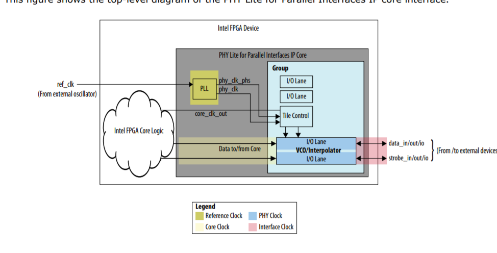
The PHY Lite for Parallel Interfaces IP core uses a reference clock that is sourced from
a dedicated clock pin to the PLL inside the IP core.
Reference Page no: 10
https://www.intel.com/content/dam/www/programmable/us/en/pdfs/literature/ug/ug_altera_phylite.pdf
Attaching the IP block diagram for your reference, it is clearly mentioned to connect to reference clock source.
Try to connect the input clock pin to phylite directly to input pin , the design you send is working correctly when connected to the dedicated input.
- Als neu kennzeichnen
- Lesezeichen
- Abonnieren
- Stummschalten
- RSS-Feed abonnieren
- Kennzeichnen
- Anstößigen Inhalt melden
Hi ,
Kindly let me know , you need further assistance
- Als neu kennzeichnen
- Lesezeichen
- Abonnieren
- Stummschalten
- RSS-Feed abonnieren
- Kennzeichnen
- Anstößigen Inhalt melden
Hi ,
If you do not have further query , kindly let me know can I close the thread
- RSS-Feed abonnieren
- Thema als neu kennzeichnen
- Thema als gelesen kennzeichnen
- Diesen Thema für aktuellen Benutzer floaten
- Lesezeichen
- Abonnieren
- Drucker-Anzeigeseite