- Mark as New
- Bookmark
- Subscribe
- Mute
- Subscribe to RSS Feed
- Permalink
- Report Inappropriate Content
Has anyone have a working Simple Socket Server (SSS) design for the Stratix III development kit for Quartus 11.1 (or 12.x or 13.x) that they are willing to share? I am seeking a hardware design for Quartus and software for the Nios II (via Eclipse) that function together.
I have made numerous attempts trying to use the Standard Nios II hardware design for the Stratix III dev kit using the files provided in the Quartus v11.1 kit installation here: https://www.altera.com/products/boards_and_kits/dev-kits/altera/kit-siii-host.html. After trying to work with the original design, I rewrote that hardware design from scratch in Qsys since the design I downloaded had older IP for the PLL. The Standard design in Qsys contains the following components: -Nios II processor -onchip_memory -tristate conduit bridge (to ext_flash) -tristate conduit pin sharer (connects to ext_flash and maxii_interface) -ext_flash -maxii_interface -reset bridge -sys_clk_timer, high_res_timer -sys_pll -jtaguart -led_pio, button_pio -sysid -sdram (DDR2 DIMM using UniPHY) -osc_clk -sgdma_tx, sgdam_rx -tse_mac (triple speed ethernet mac) -descriptor_memory (additional onchip ram) I have tried using various versions of the simple socket server software, since it seems those software files need to be tweaked for the particular board. Most typically when I run my hardware design using simple socket server files in Eclipse, the project builds but I get a "m_state == STATE_DEBUG" error like shown in this screenshot: http://www.alteraforum.com/forum/attachment.php?attachmentid=12503&stc=1 I have successfully been able to run the external memory with UniPHY tutorial (https://www.altera.co.jp/ja_jp/pdfs/literature/hb/external-memory/emi_tut_qdr.pdf) so I am reasonably confident that the external memory interface works correctly. I found this design for the Stratix III dev kit (in the second post of this forum thread http://www.alteraforum.com/forum/showthread.php?t=5886), but the design was made for Quartus/Nios II EDS 8.0 and does not work with Nios II EDS 11.1. Does anyone have any suggestions for a newbie like me about how to determine what components should or should not be in my hardware design? And how can I determine version of the SSS software files I should use or how I should modify the software files for my hardware? I am relatively new to FPGA, and I am self-taught. My understanding of exactly what is going on in the SSS software files is limited, so any suggestions on how to tackle understanding that code would be helpful too. Erin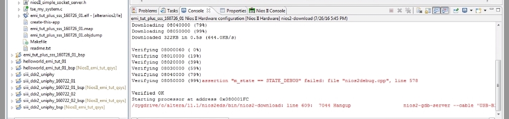
Link Copied
2 Replies
- Mark as New
- Bookmark
- Subscribe
- Mute
- Subscribe to RSS Feed
- Permalink
- Report Inappropriate Content
The problem you have is not related to the specific SSS software. You definitely have some issue with the JTAG connection to the device.
It could be due to electrical noise/bad grounding, timing problem or even a flaw in your design. Try googling m_state STATE_DEBUG keywords for some hints.- Mark as New
- Bookmark
- Subscribe
- Mute
- Subscribe to RSS Feed
- Permalink
- Report Inappropriate Content
Thanks for the suggestions, Cris72. I also got some useful suggestions from Deshi at Altera mySupport.
I figured out that my issue was with the hardware design. The top level file I had copied from the stratixIII_dev_niosII_standard design, and then modified, but I failed to notice that the clocks pins to the external memory (mem_ck[*] in my design) were set as bidirectional pins, but they should be output pins. I should have checked that top level file more closely and compared to the working external memory design that I have. Simple socket server now works as expected! Hooray! That success was a long time coming.
Reply
Topic Options
- Subscribe to RSS Feed
- Mark Topic as New
- Mark Topic as Read
- Float this Topic for Current User
- Bookmark
- Subscribe
- Printer Friendly Page