- Mark as New
- Bookmark
- Subscribe
- Mute
- Subscribe to RSS Feed
- Permalink
- Report Inappropriate Content
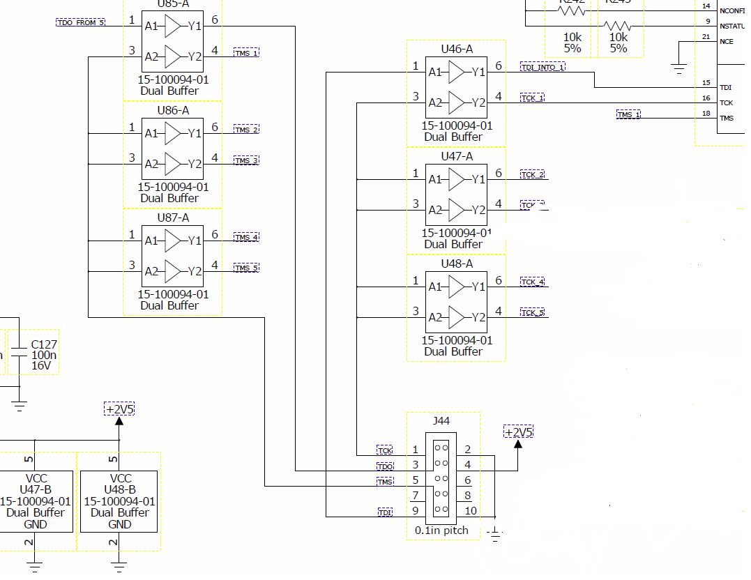
If there are multiple FPGAs on the JTAG chain, altera recommends using JTAG buffer chip on TMS, TCK and TDI pins. I could not find a proper schematic for this.
Anyone can help?Link Copied
2 Replies
- Mark as New
- Bookmark
- Subscribe
- Mute
- Subscribe to RSS Feed
- Permalink
- Report Inappropriate Content
- Mark as New
- Bookmark
- Subscribe
- Mute
- Subscribe to RSS Feed
- Permalink
- Report Inappropriate Content
I think you used the voltage supply for the buffer chip as 2.5V.
I created a similar schematic using the buffer chip 74LVC541ADB but it did not correctly work. The voltage supply for the buffer chip was 3V. Please check my thread http://www.alteraforum.com/forum/showthread.php?t=53823
Reply
Topic Options
- Subscribe to RSS Feed
- Mark Topic as New
- Mark Topic as Read
- Float this Topic for Current User
- Bookmark
- Subscribe
- Printer Friendly Page