- Mark as New
- Bookmark
- Subscribe
- Mute
- Subscribe to RSS Feed
- Permalink
- Report Inappropriate Content

 ce!
ce! - Mark as New
- Bookmark
- Subscribe
- Mute
- Subscribe to RSS Feed
- Permalink
- Report Inappropriate Content
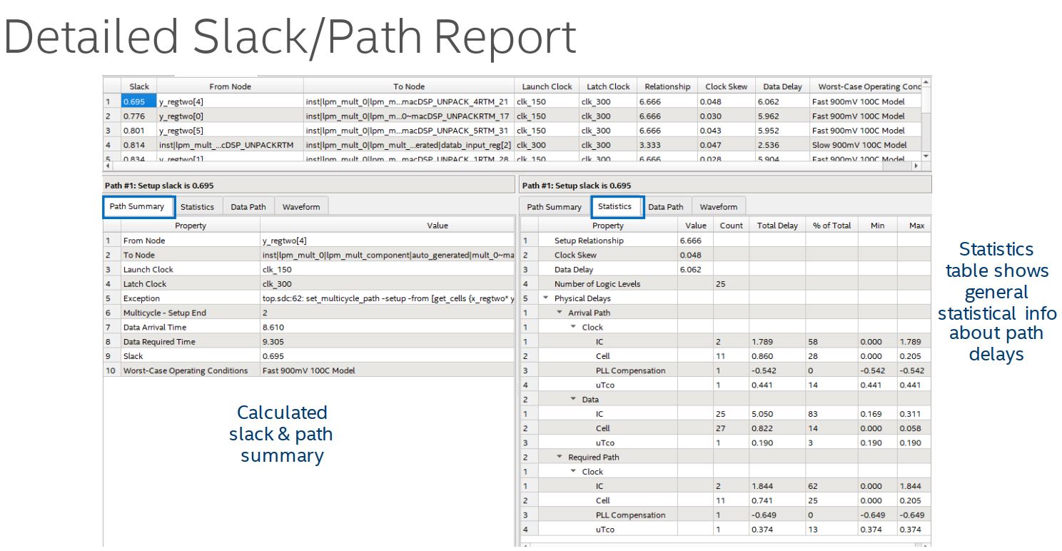
Your screenshots are not showing the whole picture (scroll to the bottom to get the data arrival and data required times; you've highlighted the clock edges, not the arrival and required times). Look at the Waveform tab in the timing analyzer reports. They show where the data arrival and data required times are located. Then correlate that to the numbers in the path reports in the Data Path tab.
Also check out this training: https://cdrdv2.intel.com/v1/dl/getContent/653046
Link Copied
- Mark as New
- Bookmark
- Subscribe
- Mute
- Subscribe to RSS Feed
- Permalink
- Report Inappropriate Content
Your screenshots are not showing the whole picture (scroll to the bottom to get the data arrival and data required times; you've highlighted the clock edges, not the arrival and required times). Look at the Waveform tab in the timing analyzer reports. They show where the data arrival and data required times are located. Then correlate that to the numbers in the path reports in the Data Path tab.
Also check out this training: https://cdrdv2.intel.com/v1/dl/getContent/653046
- Mark as New
- Bookmark
- Subscribe
- Mute
- Subscribe to RSS Feed
- Permalink
- Report Inappropriate Content
As sstrell mentioned, if you click on the Waveform tab, it will help you to visualize how the timing slack is calculated.
The Data Path tab traces timing paths through the FPGA so you will only see the exact Data Arrival Time(DAT) and the Data Required Time(DRT) at the table's last row. You can find the DAT and DRT at the Path Summary tab as well.
Attached screenshot for clearer understanding.
Best Regards,
Richard Tan
p/s: If you find any answers from the community or Intel Support to be helpful, we encourage you to mark them as the best answer or rate them 4/5 in the survey
- Mark as New
- Bookmark
- Subscribe
- Mute
- Subscribe to RSS Feed
- Permalink
- Report Inappropriate Content
Thank you for acknowledging the solution provided. I'm glad to hear that your question has been addressed.
Now, I will transition this thread to community support. If you have any further questions or concerns, please don't hesitate to reach out.
Thank you and have a great day!
Best Regards,
Richard Tan
- Mark as New
- Bookmark
- Subscribe
- Mute
- Subscribe to RSS Feed
- Permalink
- Report Inappropriate Content
Understanding setup and hold timing in FPGA design can indeed be challenging, and you're not alone in facing these difficulties. The formula you mentioned is correct, but the devil is often in the details. Let me provide some clarification and references to Intel's Quartus Prime Timing Analysis manual.
Setup Slack: It's the time difference between the required time for data to stabilize (Setup) and the actual arrival time of the data. Mathematically, Setup Slack = Data Required Time (Setup) - Data Arrival Time.
Hold Slack: It's the time difference between the actual arrival time of the data and the required time for the data to remain stable (Hold). Mathematically, Hold Slack = Data Arrival Time - Data Required Time (Hold).
It's important to note that negative slack values indicate a violation of timing constraints, meaning your design may not meet the required timing specifications.
For detailed insights and step-by-step guidance on calculating setup and hold slack using Intel Quartus Prime, I recommend referring to the official documentation. Check the Timing Analysis chapter in the Intel Quartus Prime Handbook, particularly the section on Setup and Hold Timing Analysis.
Additionally, online tools and calculators specific to FPGA timing analysis might be beneficial. Intel's forums and community support are also excellent resources for getting help with specific challenges you're facing.
Remember, FPGA timing analysis concepts often become clearer with practice, so don't hesitate to work through examples and seek community assistance. Best of luck with your FPGA design endeavors!
Reviewed by https://gstcalculatoronline.com/australian-gst-calculator/
- Subscribe to RSS Feed
- Mark Topic as New
- Mark Topic as Read
- Float this Topic for Current User
- Bookmark
- Subscribe
- Printer Friendly Page