- 新着としてマーク
- ブックマーク
- 購読
- ミュート
- RSS フィードを購読する
- ハイライト
- 印刷
- 不適切なコンテンツを報告
OK I've decided to go with Block Design Files approach to programming a IV Cyclone in Quartus. Seems easier than Verilog from scratch to me. My application has lots of pins but is fairly simple.
There is one catch however, I’m interfacing a number of the FPGA pins to an external bidirectional bus. Straight in & out pins are obvious. For bidirectional I assume I use a symbol alt_outbuf_tri. Under “Symbol Properties/ports it has 3 names i, o, and oe. It’s unclear to me how I access/connect up to the oe port with wires. The oe does not appear in the schematic I assume I somehow raise (or lower) oe before reading in from the FPGA actual pin to inactivate the gates output and do the opposite when writing to the FPGA pin only this time drive the signal through the gate. Can somebody point me to a .bdf file with FPGA pins interfaced to an external bidirectional pin or provide a simple picture. Thanks in advance for helping somebody just getting started.コピーされたリンク
2 返答(返信)
- 新着としてマーク
- ブックマーク
- 購読
- ミュート
- RSS フィードを購読する
- ハイライト
- 印刷
- 不適切なコンテンツを報告
Hi,
--- Quote Start --- For bidirectional I assume I use a symbol ALT_OUTBUF_TRI. Under “Symbol Properties/ports it has 3 names i, o, and oe. It’s unclear to me how I access/connect up to the oe port with wires. The oe does not appear in the schematic --- Quote End --- Check screenshot, You can see the “oe” port. Refer following thread as well for reference, https://www.alteraforum.com/forum/showthread.php?t=38718 Let me know if this has helped resolve the issue you are facing or if you need any further assistance. Best Regards Vikas Jathar (This message was posted on behalf of Intel Corporation)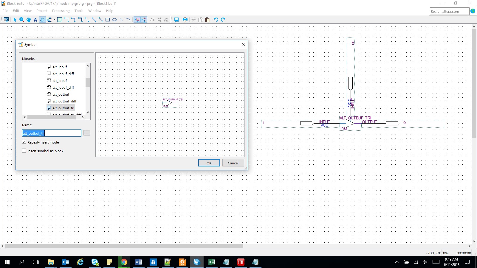
- 新着としてマーク
- ブックマーク
- 購読
- ミュート
- RSS フィードを購読する
- ハイライト
- 印刷
- 不適切なコンテンツを報告
Thanks jatharvk, that did the trick. I later found I can use 74xxx chips from the ..others/maxplus2 library and use two 74373b "chips" for an internal 8 bit bidirectional library in one shot.
very impressive! simple, quick!.