- Mark as New
- Bookmark
- Subscribe
- Mute
- Subscribe to RSS Feed
- Permalink
- Report Inappropriate Content
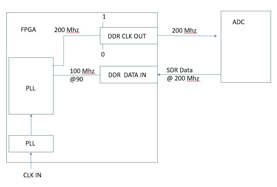
In the design in question, I have two clocks generated from a PLL and thus have a known phase relationship, The one clock, CLK_OUT clocks a DDR output with its D inputs tied to 1 and 0, thus recreating and forwarding the clock out to an ADC. The other clock, CLK_IN, clocks in the incoming samples, ADC_DATA from the ADC.
The ADC sends samples back to the FPGA with an known timing relative to CLK_OUT, and hence a known relationship to CLK_IN. Furthermore the board delays, ADC delays, and so forth are known and included into the input delay spec as required.
At issue is which clock to use in the input delay spec. I have tried using CLK_OUT as the clock source in the input constraint, but get weird results, in that when performing "Report All IO Timing" the ADC_DATA pins do not show up in the report.
I created a virtual clock CLK_OUT_virt, with the appropriate period, and use that in the input constraint, and the IO now appear in the IO timing report, but the phase relationship between the launching and latching clocks is not correct.
- Mark as New
- Bookmark
- Subscribe
- Mute
- Subscribe to RSS Feed
- Permalink
- Report Inappropriate Content
The virtual clock you need should really be CLK_IN_virt, the clock that is driving the ADC to generate the data incoming to the FPGA. Are you saying that the output clock from the FPGA is what is controlling this? If so, this is referred to as a data feedback design. The SDC should look something like this:
# define input and pll clocks
create_clock –name clk_in –period 10.00 [get_ports clk_in]
derive_pll_clocks

# define generated output clock to be used as ASSP clock
create_generated_clock –name clk_out -source [get_pins {pll|clk[0]}] /
	[get_ports clk_out]

# define false path on output clock port
set_false_path –to [get_ports clk_out]

# define input delay constraints based on clk_out from FPGA
set_input_delay –clock clk_out –max 6 [get_ports datain*]
set_input_delay –clock clk_out –min 2 [get_ports datain*]
CLK_OUT becomes the launch edge for the incoming data and the 100 MHz clock capturing the incoming data becomes the latch edge. Replace the input delay values as appropriate.
#iwork4intel
Link Copied
- Mark as New
- Bookmark
- Subscribe
- Mute
- Subscribe to RSS Feed
- Permalink
- Report Inappropriate Content
- Mark as New
- Bookmark
- Subscribe
- Mute
- Subscribe to RSS Feed
- Permalink
- Report Inappropriate Content
The virtual clock you need should really be CLK_IN_virt, the clock that is driving the ADC to generate the data incoming to the FPGA. Are you saying that the output clock from the FPGA is what is controlling this? If so, this is referred to as a data feedback design. The SDC should look something like this:
# define input and pll clocks
create_clock –name clk_in –period 10.00 [get_ports clk_in]
derive_pll_clocks

# define generated output clock to be used as ASSP clock
create_generated_clock –name clk_out -source [get_pins {pll|clk[0]}] /
	[get_ports clk_out]

# define false path on output clock port
set_false_path –to [get_ports clk_out]

# define input delay constraints based on clk_out from FPGA
set_input_delay –clock clk_out –max 6 [get_ports datain*]
set_input_delay –clock clk_out –min 2 [get_ports datain*]
CLK_OUT becomes the launch edge for the incoming data and the 100 MHz clock capturing the incoming data becomes the latch edge. Replace the input delay values as appropriate.
#iwork4intel
- Subscribe to RSS Feed
- Mark Topic as New
- Mark Topic as Read
- Float this Topic for Current User
- Bookmark
- Subscribe
- Printer Friendly Page
