- Mark as New
- Bookmark
- Subscribe
- Mute
- Subscribe to RSS Feed
- Permalink
- Report Inappropriate Content
Hi all,
I have a board that configured the Cyclone 4 E device JTAG signals with 2.5V with 100 ohm series resistor on all signals and TMS, TDI pulled up to 2.5V through 2.2k resistors. I observed the following waveform during quartus programmer (Quartus Prime Lite 17.1) doing an auto detect, as attached. The signals from top to bottom are TCK, TDO, TMS, and TDI. I noticed that TCK level is a bit low and TDO voltage level is unstable (not even dropping to 0V when supposed to be low; it is 0V when idle though). The effect of this is that when I downloaded sof (which is successful) with a signaltap instance, the tool reports error: invalid JTAG configuration. I suppose this is a signal integrity issue? I am using Terasic blaster right now. I see that there is a Rev. C USB blaster from Altera that is supposedly better in terms of noise issue. There is also USB Blaster II that I suppose will also work better? But it seems Rev. C is even more expansive than Blaster II. Please share your experiences working with these 3 programming cables. regards, Ben https://alteraforum.com/forum/attachment.php?attachmentid=15673&stc=1
Link Copied
- Mark as New
- Bookmark
- Subscribe
- Mute
- Subscribe to RSS Feed
- Permalink
- Report Inappropriate Content
Yes, this sounds exactly like a signal integrity issue. The newer Altera USB-Blaster has a flexi-rigid cable to the target instead of standard ribbon cable, like the Terasic Blaster. That is to combat exactly this issue.
I'd remove the 100R resistors - short them out. You might consider keeping a smaller value on TCK. The TDO should certainly improve without a series termination - the TDO buffer out of the FPGA is not very strong. The voltage levels you refer to being a little low could easily be your oscilloscope and probing (perhaps) not being up to the job. However, I wouldn't worry about that for the minute. Do you have particularly long JTGA traces on your board? Try changing the resistors and see if that improves things. Cheers, Alex- Mark as New
- Bookmark
- Subscribe
- Mute
- Subscribe to RSS Feed
- Permalink
- Report Inappropriate Content
Hi Alex,
The problem is this is an expensive board I purchased from Enclustra a few weeks ago. I do not want to modify it, though I would be nice to prove to them that their product is defective; but I cannot be so sure. I did try the same blaster with a working Cyclone 3 starter board. The waveforms look like the attached (exactly the same setup). https://www.alteraforum.com/forum/attachment.php?attachmentid=15688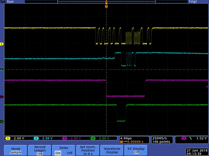
- Mark as New
- Bookmark
- Subscribe
- Mute
- Subscribe to RSS Feed
- Permalink
- Report Inappropriate Content
It's impossible to determine if there's anything wrong at all with the JTAG signals due to the low time resolution. You also don't tell if you experience an actual communication problem. The waveforms seem to show valid digital signal levels.
According to my experience, the cause for different behaviour of USB blaster versions is more in the driver impedance than the cable. Insufficient TCK signal quality, particularly ringing edges causing double clocking are observed with some boards. Often the problem can be fixed by adding a small capacitor (e.g. 15 - 22 pF) between TCK and ground near the FPGA. P.S.: I overlooked the reported error. I don't think however that it can be primarily associated with the signal level variations.- Mark as New
- Bookmark
- Subscribe
- Mute
- Subscribe to RSS Feed
- Permalink
- Report Inappropriate Content
No. What I want to show with the waveforms is the fact that TDO has low level 1V instead of 0V, which explains why the circuit marginally work with vccio=3.3V but not at all with vccio=2.5V
Plus the variation of signal level, I suspect there is data contention on these signals. According to the schematics, the JTAG signals are also connected to a system controller PLD through series resistors.- Mark as New
- Bookmark
- Subscribe
- Mute
- Subscribe to RSS Feed
- Permalink
- Report Inappropriate Content
Sorry, I didn't get the 1V TDO low level point. I won't rate it unstable, the 1V level is rather stable. It's unlikely to be caused by the FPGA or the USB Blaster. Data contention should never happen in a correctly designed JTAG chain, the USB Blaster has no means to cause it at all (TDO is input only). Defective parts are a possible explanation, but more likely it's a design fault or wrongly dimensioned resistor.
We need to look at the board schematic details. Is it a development kit (which one) or a custom design?- Mark as New
- Bookmark
- Subscribe
- Mute
- Subscribe to RSS Feed
- Permalink
- Report Inappropriate Content
- Mark as New
- Bookmark
- Subscribe
- Mute
- Subscribe to RSS Feed
- Permalink
- Report Inappropriate Content
This is a CA1 module connected to the PE1 board from Enclustra. Page 3 of CA1 shows the JTAG signals from the FPGA and the series/ pullup down resistors. Page 18 of PE1 shows the JTAG connectors and series resistors with TVS diode for ESD protection. Page 5 of PE1 shows the system controller connection.
- Mark as New
- Bookmark
- Subscribe
- Mute
- Subscribe to RSS Feed
- Permalink
- Report Inappropriate Content
A fairly unconclusive hint, but nevertheless:
I have a CA1 board (several years old) and a PE1 (from this year). I have tried to configure the CA1 board by JTAG, and also fail, but in a different way: Error (209015): Can't configure device. Expected JTAG ID code 0x020F70DD for device 1, but found JTAG ID code 0xFE0F70DD. Make sure the location of the target device on the circuit board matches the device's location in the device chain in the Chain Description File (.cdf). I do not see the strange behavior on TDO. Nevertheless, the same CA1 module can be programmed on our own base board. Up to now, I have only used the PE1 board with an AA+ module, and that did work. I set up the PE1 board according to the "Reference Design for Mercury+ PE1 Base Board User Manual". Nevertheless, because it does not behave the same as in your case, I am not 100% exclude that I configured the PE1 incorrectly for the CA1. Sorry for not checking further, but it is getting late, and am going on holiday tomorrow... Maybe we can start a user group ;-)- Mark as New
- Bookmark
- Subscribe
- Mute
- Subscribe to RSS Feed
- Permalink
- Report Inappropriate Content
I contacted Enclustra support, and they confirmed similar behaviour on TCK and TDO. With 2.5V IO voltage, their auto-detect is successful but programming fails.
- Mark as New
- Bookmark
- Subscribe
- Mute
- Subscribe to RSS Feed
- Permalink
- Report Inappropriate Content
It's been some time and I would like to give an update since I just got my custom base board for testing.
It turns out that without the system controller (another CPLD connected to the JTAG signals), and a change of the termination resistors (22R instead of 100R) near the JTAG connector solves the problem.
- Subscribe to RSS Feed
- Mark Topic as New
- Mark Topic as Read
- Float this Topic for Current User
- Bookmark
- Subscribe
- Printer Friendly Page