- Mark as New
- Bookmark
- Subscribe
- Mute
- Subscribe to RSS Feed
- Permalink
- Report Inappropriate Content
Hi
We have an existing board containing a EP4SE360F35I3 (F1152 PACKAGE). I am trying to determine the maximum input Voltage that can be safely be fed into a dedicated clock input pin (single ended). Specifically CLK8P and CLK10P. (CLK8P is bank 5C which is at 2.5V, CLK10P is bank 6C which is at 2.5V.)
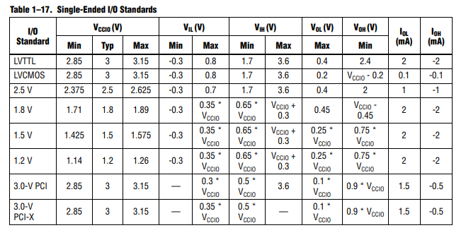
The documentation states that a single-ended clock input should be treated as IO. In which case, from the table below (for a 2.5V Vccio) the maximum 'Vih' it can safely accept is 3.6V.
If you could confirm this for me it would be greatly appreciated?
Many thanks
Simon
Link Copied
- Mark as New
- Bookmark
- Subscribe
- Mute
- Subscribe to RSS Feed
- Permalink
- Report Inappropriate Content
Hi Simon,
May I know which document/user guide you are referring? (table above)
Please provide me the link.
Thanks
- Mark as New
- Bookmark
- Subscribe
- Mute
- Subscribe to RSS Feed
- Permalink
- Report Inappropriate Content
Good morning
There seems to be a problem with the support system. I had already replied with this information but it did not appear in the support case.
The original support case has reference number 04561609, but the link in your email opens a different case without my replies in it.
Regards
Simon
**** Previous Email ****
Good morning and thank you for getting back to me.
The table was taken from the following document…
https://www.intel.com/content/dam/www/programmable/us/en/pdfs/literature/hb/stratix-iv/stx4_siv54001.pdf
Table 1-17 (Single-Ended I/O Standards) on page 1-12.
Best regards
Simon
- Mark as New
- Bookmark
- Subscribe
- Mute
- Subscribe to RSS Feed
- Permalink
- Report Inappropriate Content
Good morning
I have not heard back from you and wondered if you were able to provide an answer.The table I included in the original post was taken from the following document...
ttps://www.intel.com/content/dam/www/programmable/us/en/pdfs/literature/hb/stratix-iv/stx4_siv54001.pdf
Table 1-17 (Single-Ended I/O Standards) on page 1-12.
If you are able to advise it would be much appreciated.
Best regards
Simon
- Mark as New
- Bookmark
- Subscribe
- Mute
- Subscribe to RSS Feed
- Permalink
- Report Inappropriate Content
Hi Simon,
I'm apologize for late reply for this thread.
Yes, the User Guide you referring is the correct User Guide.
The recommended Vccio for I/O standard 2.5 V is (min 2.375, typical 2.5, max 2.625).
And if you are looking for input voltage, the table 1-17 is correct.
- VIL = minimum -0.3V, maximum 0.7V
- VIH = minimum 1.7V, maximum 3.6V
Thanks
- Mark as New
- Bookmark
- Subscribe
- Mute
- Subscribe to RSS Feed
- Permalink
- Report Inappropriate Content
Hi,
Thanks you for getting back to me.
So just to confirm, we can safely feed a single ended clock signal (maximum 3.0V) into CLK8P and CLK10P?
(Both bank 5C and 6C use a Vccio of 2.5V.)
This should be safely within the ViH limit of 3.6V as shown in the table.
Best regards
Simon
- Mark as New
- Bookmark
- Subscribe
- Mute
- Subscribe to RSS Feed
- Permalink
- Report Inappropriate Content
Hi Simon,
Yes, you're right.
You can safely feed a single ended clock signal (maximum 3.0V) into CLK8P and CLK10P.
Thanks
- Mark as New
- Bookmark
- Subscribe
- Mute
- Subscribe to RSS Feed
- Permalink
- Report Inappropriate Content
Hi
Thank you for confirming this for us.
That covers everything we need to know.
Best regards
Simon
- Subscribe to RSS Feed
- Mark Topic as New
- Mark Topic as Read
- Float this Topic for Current User
- Bookmark
- Subscribe
- Printer Friendly Page
