- Mark as New
- Bookmark
- Subscribe
- Mute
- Subscribe to RSS Feed
- Permalink
- Report Inappropriate Content
Help please. I need to write timing constraints for an SDR SDRAM for Cyclone V GX FPGA. I'm using Intel's SDRAM controller core in the design.
SDRAM that's used is AS4C4M32S-6BIN running@100 MHz (https://www.alliancememory.com/wp-content/uploads/pdf/dram/128M-AS4C4M32S-TFBGA_V3.0.pdf)
I've gone through a lot of documentation, and managed to get pretty confused (Source-Synchronous Timing with TimeQuest by Ryan Scoville, AN433, Timequest User guide, Constraining Source Synchronous Interfaces Altera Training, various forum posts... ). There are various formulas to use to determine max/min values for the IO constraints and I don't know which to use.
I don't know what the the board delays are. All the info I have are the timing diagrams from the SDRAM data sheet. How do I derive the -max and -min input/output delays from these? Is it possible to write correct constraints using only this info?
Regarding the FPGA output constraints, SDRAM provides Data/Address/Control input setup time = 1.5 ns and hold time=1 ns.
Would it be correct to write:
set_output_delay -clock virt_mem_ck_out -max 1.5 [get_ports {memory_mem_dq[*]}]
set_output_delay -clock virt_mem_ck_out -min -1 [get_ports {memory_mem_dq[*]}]
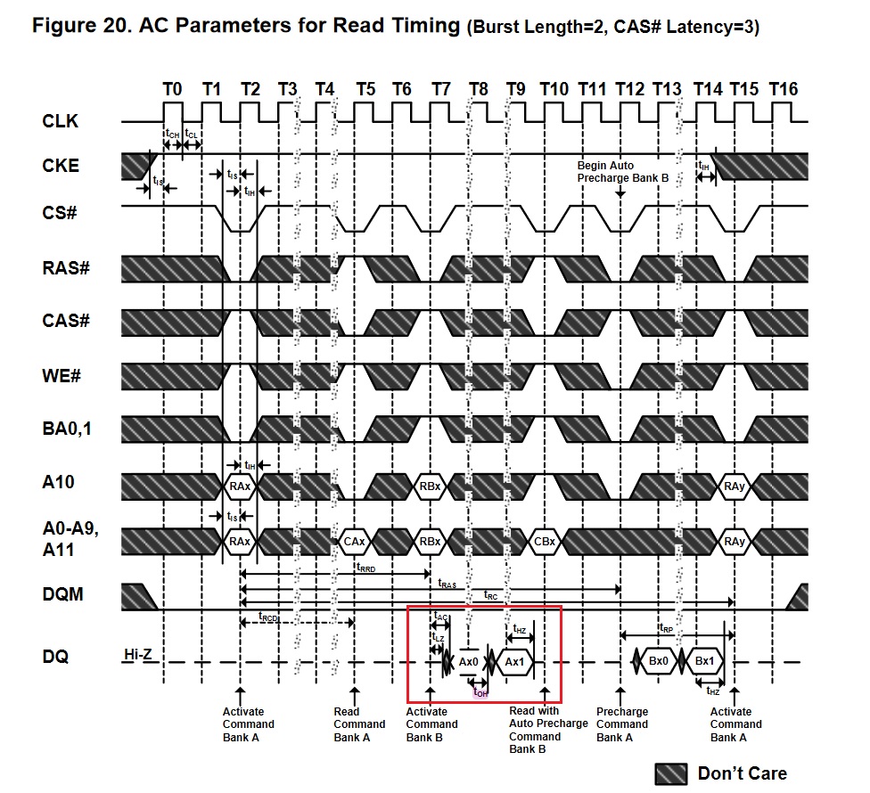
What about the input to FPGA? I attached a screenshot of a timing diagram of SDRAM read with the following timing parameters:
Access time from CLK = 6 ns
Data output hold time = 2.5 ns
Also, If I understand correctly, my DQ interfaces will be center(ish)-aligned since I will shift the SDRAM clock? Both input and output?
Another issue that's bugging me is the SDRAM clock phase shift amount.
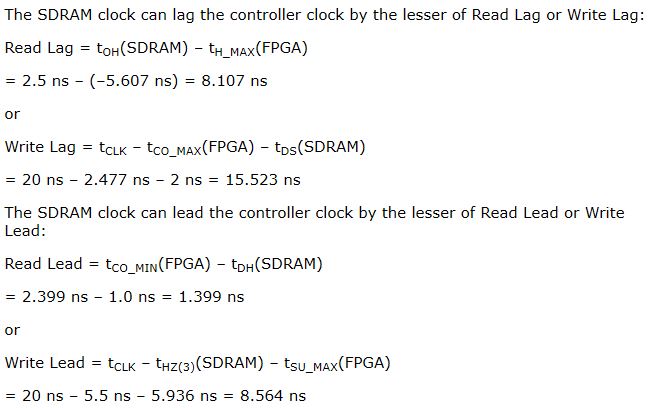
In the SDRAM controller core documentation, there's a chapter on tuning the PLL to compensate the SDRAM clock to align with the valid window (32.7.3. Estimating the Valid Signal Window of the Embedded Peripherals IP Users Guide).
It says I need to use FPGA IO timing parameters from the Timing Analyzer to do this calculation.
So, do I first write set_input_delay/set_output_delay constraints for the memory interface, and then read the FPGA Tco, TH,TSU from the datasheet report in Timequest? When the calculation is done and I phase shift the SDRAM clock accordingly, do I then need to modify the IO constraints ? Or maybe not IO constraints, but virtual clock's phase which will in turn affect the timing analysis?
I already tried checking the Tco max-min, Tsu and TH values from the datasheet report by running the fitter compilation without the IO constraints. I got weird values for Tco MAX and MIN. It was around ~10 ns (9.5 ns - 11.2 ns). Isn't this too much?? Tsu was a negative value and TH a positive one. Do I use TSU as a positive or negative value in the formulas provided in the screenshot from the controller core documentation?
Hopefully someone will take the time to help me with this.
Thank you.
Link Copied
- Mark as New
- Bookmark
- Subscribe
- Mute
- Subscribe to RSS Feed
- Permalink
- Report Inappropriate Content
Hi Ana,
May I know if there is any update on this?
- Subscribe to RSS Feed
- Mark Topic as New
- Mark Topic as Read
- Float this Topic for Current User
- Bookmark
- Subscribe
- Printer Friendly Page