- Mark as New
- Bookmark
- Subscribe
- Mute
- Subscribe to RSS Feed
- Permalink
- Report Inappropriate Content
Dear all,
I am reading SERDES Transmitter/Receiver (ALTLVDS) Megafunction User Guide. In the Design Example 2: Cyclone II ALTLVDS Using External PLL Option, both functional and timing simulations shows that it can not extract data exactly: it extacts data with shifts towards MSB. In the LVDS receiver, The parallel data is shifted two bits toward the MSB, in the Transmitter, the transmitted data is three bits shifted toward the MSB. My questions are : Is this correct? In the real situations, how we know how many bits the data shifts so that the data is not corrupted? I attached the figure from the guide. Thank you very much!
Link Copied
6 Replies
- Mark as New
- Bookmark
- Subscribe
- Mute
- Subscribe to RSS Feed
- Permalink
- Report Inappropriate Content
Hi,
In a serdes data can be misaligned. You don't know that unless you have a synchonisation mechanisme besides the serdes or use a sync pattern and the bit-slip function of the serdes. Once aligned, it stays aligned. The text coming with this example is not correct. rx_in1 receives a value of 0x01, shifted 2 bits is 0x04 rx_in2 receives a value of 0x02, shifted 2 bits is 0x08 rx_in1 receives a value of 0x06 (not 3), shifted 2 bits is 0x18 rx_in2 receives a value of 0x04, shifted 2 bits is 0x10 That's the value you see at rx_parallel_out. I don't get the TX part. First of all, tx_out3 is sent in another slow_clock period than tx_out2, tx_out1 and tx_out0. So you transmit: 00000000 00000000 04000000 00030201 00000000 Also in this timing diagram there's a phase shift between clk1 out of the PLL and slow_clock, which should the the same signal, accoring to figure 2-14 of the same document. I don't see the three position data shift, but that could be me :-) Cheers, Ton- Mark as New
- Bookmark
- Subscribe
- Mute
- Subscribe to RSS Feed
- Permalink
- Report Inappropriate Content
--- Quote Start --- In a serdes data can be misaligned. You don't know that unless you have a synchonisation mechanisme besides the serdes or use a sync pattern and the bit-slip function of the serdes. --- Quote End --- Sending a correctly aligned reference clock with the data should be sufficient for synchronization. I must confess however, that I don't completely understand the alignment scheme of the Cyclone "soft" ALT_LVDS core as described in the MegaFunction manual. Also, I'm under the impression that it doesn't allow to adjust the receiver phase as required to handle all possible situations. Instead of further evaluating it's properties by trial-and-error method, I prefer to use simple self written LVDS units for Cyclone series FPGA. But "that could be me".
- Mark as New
- Bookmark
- Subscribe
- Mute
- Subscribe to RSS Feed
- Permalink
- Report Inappropriate Content
Frank, you're right. There's a lot of trial-and-error involved when using C3 (soft) altlvds_rx, with bit-slipping and phase-shifting, not to mention the problems with the buffer implementation when using an odd deserialization factor. After all I managed to get it working with an aligned reference clock and a mux buffer implementation.
Regards, Ton- Mark as New
- Bookmark
- Subscribe
- Mute
- Subscribe to RSS Feed
- Permalink
- Report Inappropriate Content
Could you give us some notes/examples on how to do that so that we can avoid some errors?
Thank you very much! --- Quote Start --- Frank, you're right. There's a lot of trial-and-error involved when using C3 (soft) altlvds_rx, with bit-slipping and phase-shifting, not to mention the problems with the buffer implementation when using an odd deserialization factor. After all I managed to get it working with an aligned reference clock and a mux buffer implementation. Regards, Ton --- Quote End ---- Mark as New
- Bookmark
- Subscribe
- Mute
- Subscribe to RSS Feed
- Permalink
- Report Inappropriate Content
Hi,
First of all: avoid odd serialization factors. That makes life a lot easier. What I did for correct synchronization is to forward the slow clock with the data, instead of the pixelclock. On the receiving side I reconstruct the pixel clock with a PLL (C0). PLL output C1 is the slow clock frequency, with a phase shift. Shift in steps of 36 degrees (=360/ serialization factor) to find the correct synchronization and leave it there. The transmitter is not in the schematic. Clock the data into the transmitter with the slow clock. Make sure the transmitter side is up-and-running before the receiver is. You may use the transmitter PLL locked output as an areset for the receiver PLL, if you have a spare signal line available. I don't think this is the best implementation with respect to jitter perfromance, but it works for me. This implementation is a simplified version of the one I use. I didn't test it. So use it without any warranty from my side. Success, Ton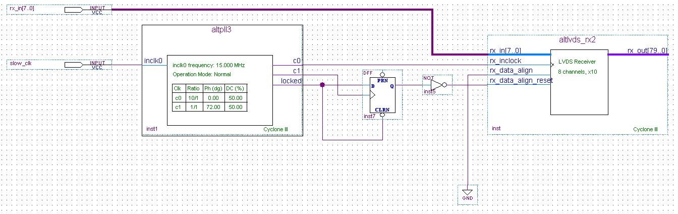
- Mark as New
- Bookmark
- Subscribe
- Mute
- Subscribe to RSS Feed
- Permalink
- Report Inappropriate Content
Two additional remarks:
- Because CIII has DDIO, C0 has to be 5/1 not 10/1 in this example. - Make sure the edges of C0 are center-aligned with respect to the data. Adapt the phase of C0 when neccesary. Regards, Ton
Reply
Topic Options
- Subscribe to RSS Feed
- Mark Topic as New
- Mark Topic as Read
- Float this Topic for Current User
- Bookmark
- Subscribe
- Printer Friendly Page