- Als neu kennzeichnen
- Lesezeichen
- Abonnieren
- Stummschalten
- RSS-Feed abonnieren
- Kennzeichnen
- Anstößigen Inhalt melden
In my simulations, some memory reads are next cycle, some are in two cycles, which is causing problems. Shouldn't it always be a consistent single-cycle with on-chip mem? I've attached a screen shot.
State is given in blue at the top. State 0: I give addresses (120, 121, then 120 again), and we see by my arrows that the readdata is return the next cycle as expected. State 1+: I switching the address to another value source. We see that it takes TWO cycles for on-chip memory to return. I've never seen this before. The verilog used is below: reg [8:0] node_pointer; // calculated value reg [3:0] node_offset; // calculated value wire [12:0] avs_s0_address;// input from other module assign avm_s0_address = switch_condition ? node_pointer * 10 + node_offset : avs_s0_address[12:4] * 10 + avs_s0_address[3:0]; The switched condition is registered, but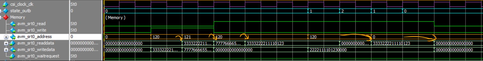
Link kopiert
2 Antworten
- Als neu kennzeichnen
- Lesezeichen
- Abonnieren
- Stummschalten
- RSS-Feed abonnieren
- Kennzeichnen
- Anstößigen Inhalt melden
This is weird. If it is supposed to take more than one cycle, I would expect waitrequest to go high, but it isn't. What is the slave component and what are its properties/parameters set to?
- Als neu kennzeichnen
- Lesezeichen
- Abonnieren
- Stummschalten
- RSS-Feed abonnieren
- Kennzeichnen
- Anstößigen Inhalt melden
sstrell,
The slave component is a generic On-Chip Memory RAM: 2-Port, exported from the Quartus IP Catalog. With two read/write ports, Q_a output as 64-bit words, Depth is 512 words, Auto memory type, Single Input clock, No byte enable or read enable, Registered read output ports q_a and q_b Asynchronous clear supported, Don't care on mixed port read during write, Same port read during write is new data, Initialize to blank. As you can see all the settings are normal. The read is one cycle before incrementing the state. Would it be a problem ifthe source address is registered? After State_1, the address is derived from a register. Still I don't see why there's a two cycle delay. On the Avalon-MM Master, the following is given. It seems to be the address port that is causing the problem: registers wires The actual verilog code: assign avm_srt1_address = f_find_op_inb ? node_pnt_inb * 10 + node_offset_inb : avs_s1_address[4 +:9 ] * 10+ avs_s1_address[3:0]; assign avm_srt1_read = f_find_op_inb ? 1'b1 : avs_s1_read; // seems to have no affect on the delay assign avm_srt1_write = f_find_op_inb ? 1'b0 : avs_s1_write; // seems to have no affect on the delay assign avm_srt1_writedata = avs_s1_writedata[63:0]; // seems to have no affect on the delay assign node_pnt_inb = {row_pnt_inb, column_pnt_inb[5:0]}; assign column_pnt_inb = check_hit[5:0]; check_hit = (!skip_array[ 0 ] & (target == search_string[ 0 ])) ? {1'b1, 8'd 0 } : (!skip_array[ 1 ] & (target == search_string[ 1 ])) ? {1'b1, 8'd 1 } : (!skip_array[ 2 ] & (target == search_string[ 2 ])) ? {1'b1, 8'd 2 } : (!skip_array[ 3 ] & (target == search_string[ 3 ])) ? {1'b1, 8'd 3 } : (!skip_array[ 4 ] & (target == search_string[ 4 ])) ? {1'b1, 8'd 4 } : (!skip_array[ 5 ] & (target == search_string[ 5 ])) ? {1'b1, 8'd 5 } : 9'b0; ... always @ (posedge csi_clock_clk or posedge csi_clock_reset) begin if(csi_clock_reset) begin ... end else begin case (state) ...... STATE_INB_IDLE: begin node_offset_inb <= '{default:0}; row_pnt_inb <= '{default:0}; ...... STATE_READ_NEXT: begin node_offset_inb <= node_offset_inb +1; row_pnt_inb <= row_pnt_inb +1;
Antworten
Themen-Optionen
- RSS-Feed abonnieren
- Thema als neu kennzeichnen
- Thema als gelesen kennzeichnen
- Diesen Thema für aktuellen Benutzer floaten
- Lesezeichen
- Abonnieren
- Drucker-Anzeigeseite