- Mark as New
- Bookmark
- Subscribe
- Mute
- Subscribe to RSS Feed
- Permalink
- Report Inappropriate Content
I have a Cyclone V FPGA interfaced with an external synchronous (ZBT) SRAM. The FPGA is clocked with a 100 MHz XO, which is passed through the FPGA and forwarded/outputted to my SRAM as its clock. Obviously the FPGA has an address-bus connected (output) to the SRAM and a bidirectional data-bus from/to the SRAM.
The relevant constraints I've used are:
create_clock -name "clk_100_in" -period 10.000ns -waveform { 0.000 5.000 } [get_ports {clk_100_in}]
create_generated_clock -name {sram_clk_out} -source [get_ports {clk_100_in}] [get_ports {sram_clk_out}]

# SRAM input minimum delay in ns
set_input_delay -clock sram_clk_out -min 1.3 [get_ports {sram_data36_inout*}]

# SRAM input maximum delay in ns
set_input_delay -clock sram_clk_out -max 3 [get_ports {sram_data36_inout*}]

# SRAM output minimum delay (=hold time) in ns
set_output_delay -clock sram_clk_out -min -0.5 [get_ports {sram_address21_out*}]
set_output_delay -clock sram_clk_out -min -0.5 [get_ports {sram_data36_inout*}]

# SRAM output maximum delay (=setup time) in ns
set_output_delay -clock sram_clk_out -max 1.5 [get_ports {sram_address21_out*}]
set_output_delay -clock sram_clk_out -max 1.5 [get_ports {sram_data36_inout*}]
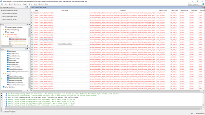
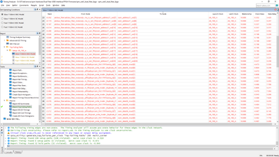
The problem is that I get consistent timing failures with the inputs for my SRAM->FPGA data-bus like this:
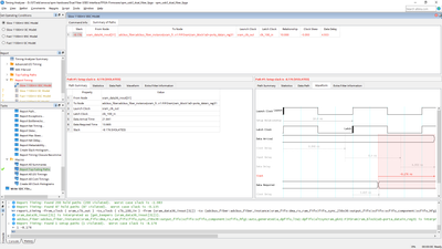
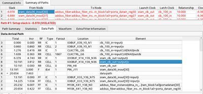
When I report the timing for eg. data[31] I get:
I think one of the issues I'm facing is the negative clock skew but I have no idea how to fix that. I've tried about a ton of things for several days now to get timing closure but I'm at a complete loss since I'm out of ideas. Any help would be greatly appreciated.
- Mark as New
- Bookmark
- Subscribe
- Mute
- Subscribe to RSS Feed
- Permalink
- Report Inappropriate Content
Sorry for the delay in response. Been taking some time to solve the timing violation.
For bidirectional I/O, they are analyzed as inputs and outputs, so they usually have both set_input_delay and set_output_delay assignments.
These sdc below in the project could be reason we got the huge negative slack. The tool analyze that the Data Arrival Path goes from clk_100_in -> sram_clk_out -> sram_clk_inout (o) -> external device -> sram_clk_inout (i) and then back to RAM block. This make it a very long timing path.
set_input_delay -clock sram_clk_out -min 1.3 [get_ports {sram_data36_inout*}]

set_input_delay -clock sram_clk_out -max 3 [get_ports {sram_data36_inout*}]
With that, I create a virtual clock and add the input and output delay constraint to the sram_data36_inout*:
create_clock -name {sram_clk_ext} -period 10.000ns

set_input_delay -clock sram_clk_ext -min 1.3 [get_ports {sram_data36_inout*}]
set_input_delay -clock sram_clk_ext -max 3 [get_ports {sram_data36_inout*}]

set_output_delay -clock sram_clk_out -min 1.3 [get_ports {sram_data36_inout*}]
set_output_delay -clock sram_clk_out -max 3 [get_ports {sram_data36_inout*}]
I also disable all the location assignment so that the fitter can place and route without being constraint, to meet the timing.
Attached the modified project. Though there is a timing violation of sram_address21_out and I believe it can be solved by tweaking the -max value to 1.0.
set_output_delay -clock sram_clk_out -max 1.0 [get_ports {sram_*_out*}]
Best Regards,
Richard Tan
Link Copied
- Mark as New
- Bookmark
- Subscribe
- Mute
- Subscribe to RSS Feed
- Permalink
- Report Inappropriate Content
The massive clock skew is definitely the problem and it's because you've defined your launch clock at the output of the FPGA, which is correct, but you've included the clock path delay through the device in the calculation. This is basically a data feedback design.
Your base clock and generated clock constraints are correct, but you need to false path to the clock output port:
set_false_path -to [get_ports sram_clk_out]
This is the same thing you do whenever you have an output clock, like if it's used for an SDR or DDR interface.
All the required data arrival components are part of the numbers you use for calculating set_input_delay max and min (clock path delay from the FPGA, the SRAM output's tco, and the data trace delay), so just removing the data analysis from the internal clock path with set_false_path (removes data path analysis but maintains clock path analysis) should do the trick.
- Mark as New
- Bookmark
- Subscribe
- Mute
- Subscribe to RSS Feed
- Permalink
- Report Inappropriate Content
Thanks for your reply. I've tried your suggestion (adding the false-path for sram_clk_out) and it doesn't seem to make any difference unfortunately. A few other things I've tried:
- I tried NOT forwarding the SRAM-clock through the FPGA (and connecting it directly from the XO to the SRAM clock input externally but that didn't fix my issue either);
- Using DCFIFO's instead of SCFIFO to allow one side to operate at clk_100_in and the other side on sram_clk_out but that didn't fix it either.
- Adding an extra input register for sram_data36_inout, again without any luck.
Do you have any other suggestions? Please note that (obviously) "clk_100_in" is also used for all the other logic in the FPGA, not just the SRAM-interface.
- Mark as New
- Bookmark
- Subscribe
- Mute
- Subscribe to RSS Feed
- Permalink
- Report Inappropriate Content
When you say adding the false path didn't make any difference, can you explain? Did you recompile the design and rerun the timing analysis? Show your updated .sdc and a detailed slack path report (including the data path and the waveform view) for a path that is still failing.
- Mark as New
- Bookmark
- Subscribe
- Mute
- Subscribe to RSS Feed
- Permalink
- Report Inappropriate Content
Yes I recompiled the design and reran the timing analysis.
My (relevant sections of) sdc now looks like:
create_clock -name "clk_100_in" -period 10.000ns -waveform { 0.000 5.000 } [get_ports {clk_100_in}]
create_generated_clock -name {sram_clk_out} -source [get_ports {clk_100_in}] [get_ports {sram_clk_out}]
# SRAM input minimum delay in ns
set_input_delay -clock sram_clk_out -min 1.3 [get_ports {sram_data36_inout*}]

# SRAM input maximum delay in ns
set_input_delay -clock sram_clk_out -max 3 [get_ports {sram_data36_inout*}]

# SRAM output minimum delay (=hold time) in ns
set_output_delay -clock sram_clk_out -min -0.5 [get_ports {sram_address21_out*}]
set_output_delay -clock sram_clk_out -min -0.5 [get_ports {sram_data36_inout*}]

# SRAM output maximum delay (=setup time) in ns
set_output_delay -clock sram_clk_out -max 1.5 [get_ports {sram_address21_out*}]
set_output_delay -clock sram_clk_out -max 1.5 [get_ports {sram_data36_inout*}]

set_false_path -to [get_ports sram_clk_out]
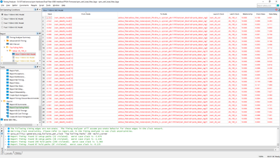
And my failing paths now look like:
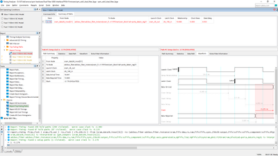
and d31's timing report looks like:
Let me know in case you need additional info. I have a feeling Quartus is having a hard time getting the timing right for sram_data36_inout input-path vs. output-path. What do you think?
- Mark as New
- Bookmark
- Subscribe
- Mute
- Subscribe to RSS Feed
- Permalink
- Report Inappropriate Content
Could you try using the constraints based on the user guide below and check if it resolves the issue?
Best Regards,
Richard Tan
p/s: If you find any answers from the community or Intel Support to be helpful, we encourage you to mark them as the best answer or rate them 4/5 in the survey.
- Mark as New
- Bookmark
- Subscribe
- Mute
- Subscribe to RSS Feed
- Permalink
- Report Inappropriate Content
Thanks for your reply but unfortunately it doesn't work and even seems to make things worse for additional signals:
I'm surprised it so complicated to get timing right for something that seems quite common (source synchronous design with a 100MHz clock). I assume there are plenty of folks out there that pair synchronous SRAMs with FPGAs, right?
- Mark as New
- Bookmark
- Subscribe
- Mute
- Subscribe to RSS Feed
- Permalink
- Report Inappropriate Content
Could you please share your design by archiving the project (Project > Archive Project)?
This would greatly assist me in conducting a more detailed investigation.
Best Regards,
Richard Tan
- Mark as New
- Bookmark
- Subscribe
- Mute
- Subscribe to RSS Feed
- Permalink
- Report Inappropriate Content
Hi Richard,
Thanks for your reply. Of course, here you go. Hopefully you can pinpoint the issue.
Kind regards,
Arno
- Mark as New
- Bookmark
- Subscribe
- Mute
- Subscribe to RSS Feed
- Permalink
- Report Inappropriate Content
Dear Richard,
Do you have an update about my issue? Did you notice/check the qar-file I uploaded?
Thanks in advance.
Kind regards,
Arno
- Mark as New
- Bookmark
- Subscribe
- Mute
- Subscribe to RSS Feed
- Permalink
- Report Inappropriate Content
Sorry for the late reply. I took some time to debug and discuss with the team.
I have a few questions regarding the design.
1) In the Timing Analyzer Failing Path, the data arrival path seem to indicate that the data go out to the external device then back to FPGA then to RAM. is this expected behavior?
2) May I know which clock is use to send data to from FPGA to SRAM and vice versa?
3) Could you provide the block diagram or system level on the design that you plan to create?
4) May I know how you calculate the input delay ? SRAM tco, trace delay for data, trace delay for clock
Best Regards,
Richard Tan
- Mark as New
- Bookmark
- Subscribe
- Mute
- Subscribe to RSS Feed
- Permalink
- Report Inappropriate Content
Hi,
Do you able to provide the information from my previous questions?
Thanks.
Best Regards,
Richard Tan
- Mark as New
- Bookmark
- Subscribe
- Mute
- Subscribe to RSS Feed
- Permalink
- Report Inappropriate Content
Dear Richard,
Sorry for my delayed response. Here are the answers you've requested:
1) I'm not sure whether I understand your question correctly but I think the answer is yes. The data-bus to the ZBT SRAM is bidirectional so I need to constrain both outgoing and incoming data (and control signals).
2) The 100 MHz (XOSC) system clock of the FPGA is used for this. It's simply forwarded in the FPGA from "clk_100_in" to "sram_100_clkout".
3) This is a (simplified) block diagram of the (SRAM)-design I'm doing. It's pretty straightforward (imho):
4) For now I assume zero trace-delay etc. for the SRAM since the PCB design hasn't been done yet AND the SRAM will be near the FPGA so the trace delays etc. will be negligible compared to the requirements of the SRAM itself. So for now I take into account the SRAM's "Data output hold after CLK rise " which is 1.3 ns and "Data output valid after CLK rise" which is 3 ns. The sync. SRAM I'm using is a Cypress CY7C1470BV25
If you need to know anything else, let me know.
Thanks for your help.
Kind regards,
Arno
- Mark as New
- Bookmark
- Subscribe
- Mute
- Subscribe to RSS Feed
- Permalink
- Report Inappropriate Content
Sorry for the delay in response. Been taking some time to solve the timing violation.
For bidirectional I/O, they are analyzed as inputs and outputs, so they usually have both set_input_delay and set_output_delay assignments.
These sdc below in the project could be reason we got the huge negative slack. The tool analyze that the Data Arrival Path goes from clk_100_in -> sram_clk_out -> sram_clk_inout (o) -> external device -> sram_clk_inout (i) and then back to RAM block. This make it a very long timing path.
set_input_delay -clock sram_clk_out -min 1.3 [get_ports {sram_data36_inout*}]

set_input_delay -clock sram_clk_out -max 3 [get_ports {sram_data36_inout*}]
With that, I create a virtual clock and add the input and output delay constraint to the sram_data36_inout*:
create_clock -name {sram_clk_ext} -period 10.000ns

set_input_delay -clock sram_clk_ext -min 1.3 [get_ports {sram_data36_inout*}]
set_input_delay -clock sram_clk_ext -max 3 [get_ports {sram_data36_inout*}]

set_output_delay -clock sram_clk_out -min 1.3 [get_ports {sram_data36_inout*}]
set_output_delay -clock sram_clk_out -max 3 [get_ports {sram_data36_inout*}]
I also disable all the location assignment so that the fitter can place and route without being constraint, to meet the timing.
Attached the modified project. Though there is a timing violation of sram_address21_out and I believe it can be solved by tweaking the -max value to 1.0.
set_output_delay -clock sram_clk_out -max 1.0 [get_ports {sram_*_out*}]
Best Regards,
Richard Tan
- Mark as New
- Bookmark
- Subscribe
- Mute
- Subscribe to RSS Feed
- Permalink
- Report Inappropriate Content
Dear Richard,
Thank you for your reply I will test it asap. However I'm a little confused about your proposal. Is it correct that you create a virtual-clock which ONLY constrains the outputs, not the inputs? Meaning the inputs are still constrained by the forwarded/generated clock? The reason I ask this is because I haven't encountered this technique anywhere before.
Kind regards,
Arno
- Mark as New
- Bookmark
- Subscribe
- Mute
- Subscribe to RSS Feed
- Permalink
- Report Inappropriate Content
No, the virtual clock (sram_clk_ext) is used to constraints input, while the output clock (sram_clk_out) is used to constraints output. As indicated in the sdc provided in my last reply.
Best Regards,
Richard Tan
- Mark as New
- Bookmark
- Subscribe
- Mute
- Subscribe to RSS Feed
- Permalink
- Report Inappropriate Content
Thanks a lot! This indeed (finally) fixed my issue.
- Mark as New
- Bookmark
- Subscribe
- Mute
- Subscribe to RSS Feed
- Permalink
- Report Inappropriate Content
Thank you for acknowledging the solution provided. I'm pleased to know that your question has been addressed.
Now, I will transition this thread to community support. If you have any further questions or concerns, please don't hesitate to reach out.
Thank you and have a great day!
Best Regards,
Richard Tan
- Subscribe to RSS Feed
- Mark Topic as New
- Mark Topic as Read
- Float this Topic for Current User
- Bookmark
- Subscribe
- Printer Friendly Page
