- Mark as New
- Bookmark
- Subscribe
- Mute
- Subscribe to RSS Feed
- Permalink
- Report Inappropriate Content
Link Copied
- Mark as New
- Bookmark
- Subscribe
- Mute
- Subscribe to RSS Feed
- Permalink
- Report Inappropriate Content
Hi,
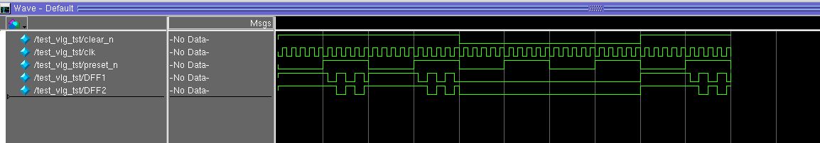
You may check the Compilation report > Timing Analyzer to see if there is any timing violation or timing related problem in the design. Besides this, do not simultaneously activate the CLEAR and PRESET inputs. You may simulate the design to verify the output of the DFF.
Thanks
Best regards,
KhaiY
- Mark as New
- Bookmark
- Subscribe
- Mute
- Subscribe to RSS Feed
- Permalink
- Report Inappropriate Content
Thank you for your reply.
In the larger design which I am trying to simulate, I see that the output of DFF with "Q" output connected directly to "D" input results in Unknown value (X) on Q output.
So, I want to know how to analyse the timing for a DFF where Q is directly connected back to D. Since I see that the output is X, I would like to know how this could be solved.
Hope my explanation is clear.
- Mark as New
- Bookmark
- Subscribe
- Mute
- Subscribe to RSS Feed
- Permalink
- Report Inappropriate Content
Hi,
Could you provide a simple test case and testbench to reproduce the behavior?
Thanks
Best regards,
KhaiY
- Mark as New
- Bookmark
- Subscribe
- Mute
- Subscribe to RSS Feed
- Permalink
- Report Inappropriate Content
Hello,
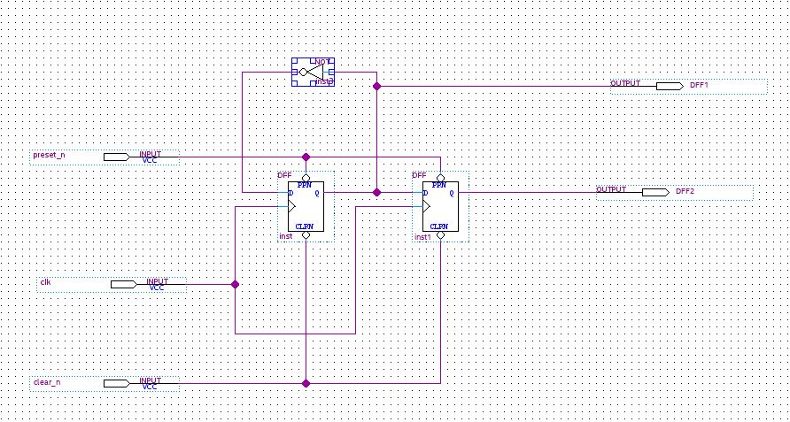
Its a large design and the test vectors are applied on top level IOs. I present the portion of schematic where I have narrowed down and found the error to be originating.

The point of interest is DFF44. Whose output is X (unknown) right from the beginning of the simulation.
CONTCLK_IN: Is the input to DFF44 and sync block.
QCLK_IN: Is the input to DFF106
Sync block is just 2 DFF synchroniser. Circuit below:

Please have a look at the simulation output. The 'X' (unknown) has propagated to sync block and later the output of OR60 block is also X. I have attached the simulation outpt for better resolution. CTEST, CLEARN and Clock inputs are all in the simulation window.
Thank you!
- Mark as New
- Bookmark
- Subscribe
- Mute
- Subscribe to RSS Feed
- Permalink
- Report Inappropriate Content
Hi,
To generate the QAR, click on Project > Archive Project > Archive.
Thanks
Best regards,
KhaiY
- Mark as New
- Bookmark
- Subscribe
- Mute
- Subscribe to RSS Feed
- Permalink
- Report Inappropriate Content
Hi,
Do you have any updates?
Thanks.
Best regards,
KhaiY
- Mark as New
- Bookmark
- Subscribe
- Mute
- Subscribe to RSS Feed
- Permalink
- Report Inappropriate Content
Hi,
Could you provide a small test case so that I could reproduce the error here?
Thanks
Best regards,
KhaiY
- Mark as New
- Bookmark
- Subscribe
- Mute
- Subscribe to RSS Feed
- Permalink
- Report Inappropriate Content
Hi,
Could provide the simple test case so that I could compile and simulate to reproduce the behavior?
Thanks
Best regards,
KhaiY
- Mark as New
- Bookmark
- Subscribe
- Mute
- Subscribe to RSS Feed
- Permalink
- Report Inappropriate Content
Hello,
Sorry for the delayed reply. I was trying to create relevant test vector inputs but was unsuccessful.
To explain the issue: The screenshot of the schematic in earlier post belongs to a file in 3rd level of instantiation. Some of the inputs to this block are generated from other blocks. Thats the reason its difficult to regenerate the behaviour without the complete project and complete set of input test vectors.
The test vectors (as mentioned earlier) are given to top level input pins.
Do you know any other way to continue solving the issue?
I can understand its difficult to answer without having the schematic and test vectors, but I would like to know if I can perform any tests as per your suggestion and post the results here.
- Mark as New
- Bookmark
- Subscribe
- Mute
- Subscribe to RSS Feed
- Permalink
- Report Inappropriate Content
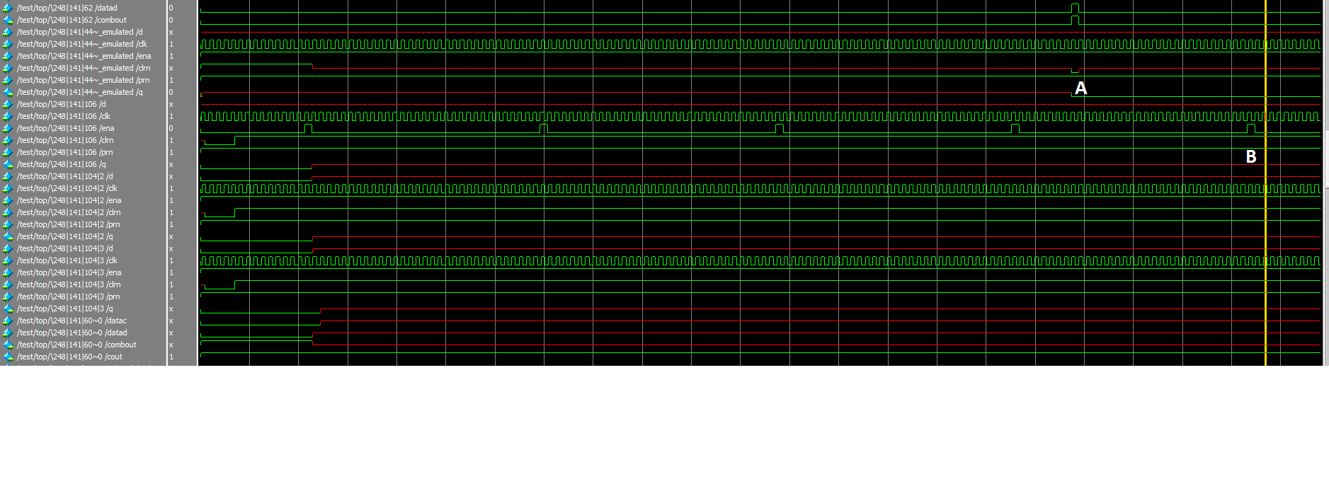
I would like to explain the flow here: Kindly refer the schematic and simulation results side by side. I have attached the simulation screenshot for better resolution. Also, the signals in simulation result are arranged in order of the data flow for easier understanding.

Starting from OR gate OR62 -> Signal levels are proper and no unknowns ('X') in sim results.
Output of OR62 given to PRN of DFF44. As D input of DFF44 is the feedback from its own output, it is understood that during the beginning of simulation, d and q of DFF44 is X.
'q' of DFF44 is directly connected to 'd' of DFFE106. The question is: at point A in simulation screenshot (marked in white colour), why doesn't the 'd' input of DFFE106 change when 'q' output of DFF44 changes to '0'?
Even after the enable signal of DFE106 is active at point B (marked in white), the change cannot be seen. Am I missing something here?
Hope the explanation is clear.
- Mark as New
- Bookmark
- Subscribe
- Mute
- Subscribe to RSS Feed
- Permalink
- Report Inappropriate Content
- Mark as New
- Bookmark
- Subscribe
- Mute
- Subscribe to RSS Feed
- Permalink
- Report Inappropriate Content
Hi,
We do not receive any response from you to the previous question/reply/answer that I have provided. This thread will be transitioned to community support. If you have a new question, feel free to open a new thread to get the support from Intel experts. Otherwise, the community users will continue to help you on this thread. Thank you.
Best regards,
KhaiY
- Subscribe to RSS Feed
- Mark Topic as New
- Mark Topic as Read
- Float this Topic for Current User
- Bookmark
- Subscribe
- Printer Friendly Page